6

So ive been playing with some Sigma Delta ADCs, for sampling low frequency (<2Khz) AC signals.

The ADC supports a differential input with a full scale value of about +-500mV at its inputs. I have constructed a reference design which consists of an input attenuation network that takes my input voltage, divides it by a factor of about a 1000 which then appears across the ADCs inputs; i also have an anti aliasing filter etc.

To play around with it, i decided to measure a few DC voltages far less than the usual full scale AC input (220v RMS) i would be using normally. What ive noticed is that there is some inherent noise from the ADCs outputs. For example, for an input of 30v DC verified to be stable, i see about 80mV noise (random, +- variations) in the readings. The noise seems to have a fundamental of about 100-200Hz.

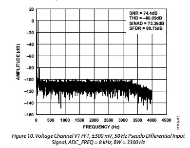
I think i understand concepts such as noise floor, quantization noise, spurs etc so I wanted to see if i could explain this; so i turned to the datasheets performance figures for the ADC and i found this:

enter image description here

I believe this explains my observations; I can see a spur about 80dB down from the reference input, around the noise frequency i observed.

Furthermore, I made a few calculations:

500mV is the full scale reference level shown in the graph, so the spur that is 80dB down, represents 50uV worth of noise at the ADCs input. As i have an attenuation network of about 1000, that translates to an equivalent value of about 50uV * 1000 = 50mV worth of noise in my input voltage. This is close to the 80mV noise figure i observed.

My question is: Is such analysis valid and could explain my observations?

PS: This question is a bit tricky to explain, please comment for additional information

EDIT 1: Here is the ADC that im talking about: datasheet
MAM
  • 1,801
  • 13
  • 24

2 Answers2

3

You have certainly started looking in the right places, and are making sensible observations, but the world of interpretting ADC specs and real world performance needs some experience.

Looking at the data sheet FFT presented, the -80dBc spur is clearly a harmonic of the 50Hz fundamental being measured. It's at the right frequency and well out of the noise floor. This will not be present when measuring DC.

More relevant is the noise floor, shown at a level around -100dBc, but this requires careful handling. The -100 is the amount of power in each FFT bin, however as we're not told the length of the FFT or (equivalently) its noise bandwidth, that's meaningless. What we do have are the summary figures in the top right of the graph, which gives SNR (signal to noise ratio) as about -74dBc. This means the total integrated noise across the DC to 4kHz bandwidth, excluding that 100Hz spur, is 74dB below the full scale fundamental power. That's double the rms voltage of a -80dBc signal.

While it's relatively easy to estimate the voltage of a signal spur, it's repetitive, a clear peak to peak, and independent of bandwidth, the same is not true of noise.

Your observation of about 80mV noise is difficult to use, on two counts. The first, the peak to peak of noise is ill-defined, and rms noise is difficult to estimate by eye. The second, what is the bandwidth of the noise? This even more difficult to estimate. Whereas a spur is independent of bandwidth, noise power has a 'per bandwidth' density.

If we assume that either you're looking at a graph of the full 8ks/s readings, or some points selected from those, then the effective bandwidth is the full 4kHz, and you would expect to see the full -74dB noise power. If any averaging is happening, explicitly or implcitly, then less.

In the context of your scaling, a -74dBc figure for noise would be rms voltage of around 100mV.

The usual practice for DC observations is to do some averaging of the points read out. This reduces the noise bandwidth, and so reduces the noise power. It's often said that averaging 2 readings together gives a 3dB improvement in SNR. This is true while the noise floor is flat.

Take a close look at the noise floor in the FFT in the range below 200Hz. The noise floor starts to lift towards DC. This is common amongst all types of semiconductors. What this means is that once your filtering has excluded all the flat noise above 200Hz, you will see less and less improvement as you reduce the bandwidth further. The effect that you see, you may interpret as 1/f noise, or at longer time scales, drift, rather than added noise.

Users and manufacturers of low noise opamps aimed at precision DC applications have a hard time interpretting noise and drift for their products, often showing time domain graphs filtered to a 0.1Hz to 10Hz bandwidth. Find and read a few data sheets for this type of product if you're interested.

Neil_UK
  • 158,152
  • 3
  • 173
  • 387
  • 1)Thankyou for you in depth and excellent explanation! Really is a treat So the idea is to represent your noise floor as an equivalent RMS voltage which is about 100mV as you said. Now, if i understand correctly, i can somewhat use this figure of 100mV to justify the DC variations that i am seeing? I understand the need to average out results, however, before doing so i wanted to make sure if DC variations of 80-100mV that i am seeing are somewhat expected, as frankly i assumed the ADC would be better given the high resolution available. 2) can you explain how you got to 100mV RMS noise? – MAM Aug 31 '16 at 11:27
  • I didn't do the sums properly, so confess may have it wrong. I took your calculation of 50mV for a -80dBc spur. The 74dB SNR is 6dB worse, or 2x worse, so I quoted 2x worse than 50mV. 74dB is a factor of 5000 (voltage), so if your ref level is 500mV, and you throw in a 1000:1 divider, that does come out at 100mV. – Neil_UK Aug 31 '16 at 11:52
  • @AdilMalik remember that the resolution of the output data says nothing about the worst-case performance of the data converter. Take a look at 'effective number of bits'. It's a tricky term that can apply to both data converters and whole systems. – user2943160 Aug 31 '16 at 12:05
  • Yes i had fallen into this trap of assumption. Calculating the ENOB comes to about 11.6 bits, which also explains it. – MAM Aug 31 '16 at 12:09
1

I prefer to look at this a little differently, though in the end, equivalently. Every ADC has a resolution, in bits. The number I like to work with is ENOB, or effective number of bits. Every ADC loses effective bits, in the ideal, due to quantization, and then there's losses of bits above and beyond that for noise.

Analog Devices has a great document on this: http://www.analog.com/media/en/training-seminars/tutorials/MT-003.pdf

It's easy to go back and forth between SINAD and ENOB, so you have this buried a bit in your datasheet.

This stuff can get pretty complicated for Sigma Delta's because of noise shaping, and thus I like really detailed treatment in a datasheet. To some extent, you can think of Sigma Delta's as oversampling and averaging, so ENOB and sample rate are related. Check out the datasheet for the ADS1263 32-bit Sigma Delta ADC from TI, paying close attention to table 1, which gives you ENOB for all sample rates, all the internal filters that can be applied, and all the issues surrounding the internal programmable gain amp. When you have a spec like that, you can then

  1. Look at the data sheet to determine if the specs meet your needs in a straightforward way, and

  2. quantify your own noise after implementation, figure out how how many bits it covers, look at your noise budget in terms of passives and amplification, and figure out if you're giving away bits of resolution above and beyond spec.

You can, of course, accomplish this with the AD datasheet, but I like to see it all laid out in black and white.

Scott Seidman
  • 29,274
  • 4
  • 44
  • 109