3

It is known that the return current starts following the conductors as the frequency increases: return current So as long as one keeps the distance between the conductors large enough there shouldn't be the need for local ground planes.
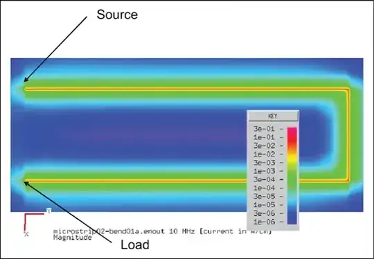
Why then some people suggest the use of localized ground plane, like the answer to this question: https://electronics.stackexchange.com/a/15143/4512 It is suggested that the ground plane will work as a patch antenna.

But the current on the ground plane will closely follow the conductor, resulting in a small loop area. And the generated magnetic field is given by Faraday's law: $$\oint_{\partial A} \mathbf{E} \cdot d\mathbf{r} = - \frac{\partial}{\partial t} \iint_A \mathbf{B} \cdot d\mathbf{s}$$

By using a smaller localized ground plane the generated EM radiation will be the same, because the loop will be the same. Additionally, the localized plane can introduce plane resonance, and one needs to avoid crossing it with high frequency signals.

So, what are the benefits of using a localized ground plane?

user110971
  • 6,067
  • 1
  • 15
  • 23

1 Answers1

6

It's not just all about loop area. Small loop area is important to reduce radiation and susceptibility, but I expect you want your circuit to do more than not radiate anything.

Currents across a ground plane cause offset voltages. That's bad since another job of a ground plane is to provide a common reference voltage to all parts of the circuit. In a purely digital circuit, you might be able to tolerate a few 100 mV offset. If the circuit contains analog components, much smaller offset could be bad.

Another problem with offsets are that they can excite the ground plane to resonate. A microcontroller in the middle of a board with part of its power/ground loop running across the ground plane can turn the whole thing into a center-fed patch antenna. The current loop may be small, but it causes voltage offsets at either end, which can cause even higher voltages at the edges due to resonance.

The more you use a ground plane, the less good of a ground plane it becomes. You have to make a tradeoff somewhere that results in the best overall characteristics taking all the competing demands into account.

Olin Lathrop
  • 310,974
  • 36
  • 428
  • 915
  • But isn't the standard solution to that to put it through FEM, e.g. ANSYS, and place enough capacitors to prevent that. I guess you can either do: split plane, or stitching capacitors. Also, in my experience, the smaller planes can actually resonate at more frequencies in your range of interest and they tend to be harder to suppress. That is because there are just more dimensions as opposed to the rectangle of the single plane. So when do you choose to do split plane instead of FEM, provided you have access to the tools? – user110971 Aug 16 '16 at 13:43
  • @user110971: The standard situation is usually to have someone experienced do a proper design and then pass EMI or whatever tests you require. Rarely do people do such analysis with FEMs as a standard step in development, at least not at low frequencies. – PlasmaHH Aug 16 '16 at 13:52
  • @user: Maybe we're talking about different frequency ranges. If you're doing deliberate high frequency RF stuff, for example, then you may have to analyze at that level. Otherwise, no, the standard solution is to use good practises and perhaps some emissions testing. I'm talking about microcontrollers with the typical analog and digital circuits around them. Smaller planes resonate at higher frequencies where there is less power in the first place. Then there is still the main ground plane anyway. I've done this successfully, as shown by RF emissions testing. – Olin Lathrop Aug 16 '16 at 13:54
  • @OlinLathrop Yes, I was thinking more FPGAs with potentially some high speed SERDES e.g. USB, PCIe etc. I should have been more precise in my original question. – user110971 Aug 17 '16 at 14:10