13

I have read here and there some articles about pcb guard trace/ring. But none of them discussed how to correctly implent it. What I could find were some pictures and comparison that cant help me at the moment!

What I would like to know is how can I make the following circuit more current-leakage proof (In design case - I know that PCB material and SIR plays a big rule).enter image description here

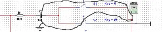
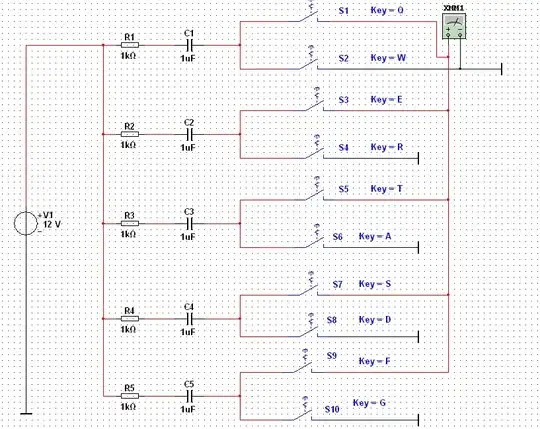
The circuit will supply up to 30V through resistors and each resistor is connected to capacitor. Each Capacitor is then connected to a switch matrix and finally single output from switch matrix is connected to a picoammeter to measure the leakage current of the capacitors.

I am wondering if I should care about leakage current in the circuit or not! If so, how can I improve it?

This is my test circuit:

enter image description here

I am thinking of connecting the capacitors just by wire into the circuit, that is one pin of capacitor soldered to by a wire in the little circuit I designed, and the other pin also with a wire soldered to BNC shield that goes to picoammeter and is in common with voltage source (SMU)

Nick Alexeev
  • 37,739
  • 17
  • 97
  • 230
Dumbo
  • 3,244
  • 14
  • 44
  • 69
  • 3
    Where do the capacitors sit in your layout? You definitely don't need a guard ring around the resistors -- current will "leak" plenty through the resistors themselves. What you do need, as I understand it, is to make sure there's no leakage path, other than the capacitor under test, between the two terminals of each capacitor, or from the switched terminal of the capacitor to ground. – The Photon Jan 10 '12 at 16:49
  • I am thinking of connecting the capacitors just by wire into the circuit, that is one pin of capacitor soldered to by a wire in the little circuit I designed, and the other pin also with a wire soldered to BNC shield that goes to picoammeter and is in common with voltage source (SMU) – Dumbo Jan 10 '12 at 20:54

4 Answers4

12

A guard ring is traditionally used to protect high impedance nodes in a circuit from surface leakage currents. The guard ring is a ring of copper driven by a low-impedance source to the same voltage as the high impedance node. This would typically be the input pin of an op-amp.

Here's an example of a classic guard ring layout for a metal can op-amp from National Semi's AN-241:

Guard ring layout

And here's an example of how it would be connected, from Analog's Analog Dialogue magazine:

guard ring schematic

The key feature is that the guard ring is connected to a node that will be driven to the same voltage as the high impedance node being protected, but with a much lower source impedance.

Note that not all vendor websites are created equal. Microchip's AN1258 recommends using the high-impedance net to create a guard ring around the low impedance nets --- don't do this.

Now to your specific case. While the undriven side of your capacitor is not strictly a low-impedance node, since the ammeter itself should provide a fairly low impedance path to ground when you're measuring, it's still going to cause measurement errors if any current should try to reach ground through that node instead of by another path. It wouldn't hurt to add a ring around the node like this:

enter image description here

Unlike in another answer, I wouldn't include the driven side of the capacitor within the ring, since that's a low impedance node, being driven to a fairly high voltage. However, you've indicated the net in question isn't even physically located on the PCB, so this advice is largely moot. Being as the high impedance net is basically floating in air, it should be well-protected from leakages in any case.

The Photon
  • 126,425
  • 3
  • 159
  • 304
  • Thanks a lot, this really discussed what I was looking for. – Dumbo Jan 11 '12 at 09:00
  • I don't understand why the non-inverting version has the ring connected to the inverting input. – endolith Nov 17 '15 at 16:20
  • @endolith, it looks like they emphasize tying the ring to a node with very little potential difference from the victim node. The inverting-input node is the lowest-impedance node that's at the same potential as the input node. – The Photon Nov 17 '15 at 17:08
3

Your power supply is DC. You wrote that you'll be measuring the output with a picoammeter. That implies that your current is in pA range. Guard ring protecting high impedance circuit is not a bad idea idea. So, what is high impedance in your schematic and what isn't? Picoammeter input, certainly is high impedance. 12V power supply, certainly isn't.

Here's how I would do it. Notice that the ring runs between the pins of R1, between the pins of S2, between the pins of the picoammeter:

enter image description here

What to connect the ring to? The guard ring has to have low impedance path to ground. The best approach is to have the guard ring at approximately the same voltage as the signal, which the ring is protecting. That way, the leakage between the signal and the ring will be small, because the voltage difference between them is small. Sometimes, connecting the ring to GND works. Sometimes, you need a guard amplifier (look it up).

-Nick

P.S. Methods for reducing DC leakage are different from those for combating conducted or radiated EMI.

Nick Alexeev
  • 37,739
  • 17
  • 97
  • 230
0

The guard ring is (somewhat) not needed. For EMI reasons you don't want to run signals or power close to the edge of the ground plane. If the signal was routed (on a different layer) up to the edge of the ground plane then there is the possibility of EMI squirting out the side. By simply not routing that signal all the way to the edge you can dramatically reduce the EMI that's spitted out. I forget the exact distance from signal to ground plane edge, but it is somewhere in the neighborhood of 0.050 inches.

Of course, this makes one wonder what to do with that 0.050 inches with nothing in it. What some PCB designers do, including me, is to put a ground trace around the perimeter of the ground plane and then tie that trace to the plane using vias approximately every 0.25". I don't honestly think this improves things over just having that gap, but it seems good in theory, doesn't hurt things, and at least provides a good reminder to not route signals there.

Power layers should be done similarly, in that they should be pulled back from the edge of the ground plane. I just go ahead and put a ground ring on the power plane layer, and tie it to ground like before. Like with the signal layers, it provides a good way to "automagically" pull the power plane back.

This method does not apply to PCB's that don't have a ground plane. Putting a ground ring around such a PCB might make things worse, not better, if that ring ends up carrying any current.

I don't believe that this will do anything for leakage, although EMI works both ways. Any circuit that radiates EMI can also receive EMI. So from this perspective it might make your design more tolerant of external EMI interference.

  • Thanks for nice info, so In my case, I shouldn't worrey about it? – Dumbo Jan 10 '12 at 20:55
  • Yup. Don't worry about it. –  Jan 10 '12 at 22:02
  • Now that you said that, I guess I should remove that trace I draw around the PCB. I am wondering what will happen it stays there? – Dumbo Jan 10 '12 at 22:04
  • 2
    @Sean87, Don't be so quick to accept an answer...give some time for others to respond. I had the idea you were asking about the type of guard ring normally used to prevent leakage into high-impedance circuits, whereas David is answering you about EMI shielding. These are not the same type of problem...and I don't think David is specifically addressing the question you asked. – The Photon Jan 10 '12 at 22:20
  • Yeah you are right...I am really confused though that what would I have to care in my case. – Dumbo Jan 10 '12 at 22:25
0

Please use the following link for this purpose:

CHAPTER 12: PRINTED CIRCUIT BOARD (PCB) DESIGN ISSUES

This will be very useful for you.

endolith
  • 28,494
  • 23
  • 117
  • 181
Syed Fahad
  • 161
  • 2
  • 1