Most likely effect is that the reset circuit is experiencing a "race condition".
Checking with a real device would be a really good idea.
TI CD4017 datasheet at
ONSEMI CD14017BD data sheet
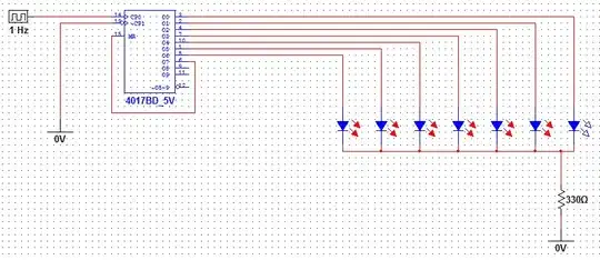
Note that as shown in your circuit the Q7 to Mr connection is strictly "illegal" and creates an 'anything can happen' race condition.
Because:
When Mr sees the reset condition it immediately starts the reset process which removes the condition causing it. The internal registers may be slower to reset than the IC is to deassert Q7 - in which case you have an undefined set of internal conditions.
Reset pulse width is 500 ns worst case at 5 V and reset to decode output propogation delay is 500 ns typical and 1 us worst case at 5V BUT has no minimum specified and is subject to capacitive and resisticvve loading ...
The counter is a 5 stage Johnson counter with 5 flip flops but 10 outputs so, unlike a stage where the are 10 flipflops which need to be rests to 0 and of which there is only one "high output" at a time, here we have a mix of on and off flipflops decoded to give a single output, and resetting some may cause (without wading through Johnson decode logic) a different and possibly unapparently related new state
Adding an RC delay in the Q7 to Mr reset circuit makes it much more likely that proper resetting will occur in practice.
Detail: An equally illegal [tm] :-) but real-world-often-better result can be achieved by connecting a resistor from Q7 to Mr and a small capacitor from Mr to ground. eg say 1k Q7-Mr and 0.1 uF Mr to ground gives a time constant of 100 us in the reset line. Mayhaps 10k and 10 nF would work as well in reality or some mix - max tolerable reset delay depends on clock speed but in your case the 1 Hz clock makes it "quite tolerant".
This ensures that a high voltage remains on Mr after it is removed from Q7.
Vih and Vil specs overlap in such a way that you cannot guarantee that if Vih is JUST reached and then falls slowly that Vih will be maintained for a small while (thus allowing reset to proceed properly) but in practice this is much much more likely with an RC delay than without one.
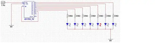
Depending how good your simulator is it may be responding to the fact that you are applying (5-VLED)/330 - V??? to all the off outputs - which can notionally cause strange results as there is no formal stat for applied voltage into the outputs. I say V??? as you have not stated LED colour or Vf and this affects the potential result.
This is very uncertain in effect as you are notionally biasing all off LEDs backwards. If they were Si diodes they would not conduct. If the were "real LEDs" they will not have major conduction until their reverse breakdown is reached = somewhat higher than here. In a model anything may happen.
Interest only - output loading:
The CD4017 max specified drive current is modest and many many users exceed it - generally with impunity, but if Murphy decides to play games you can have no complaint. In the datasheet you will see that at 5V you can draw 4.2 mA typical and 2.5 mA min at 25C with a 5V supply AND the output loaded down to 2.5V.
If Vf = 2V (red) then I LED at 5V = (5-2)/330 = 9 mA and I LED at 2.5V loaded = (2.5-2)/330 = 1.5 mA. So Voutput typical will be in the 2.5V to 5V range.