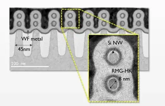
Intel and IMEC came up with multigate MOSFET designs with channels as narrow as new nanometers. Which methods/techniques/machines are used to pattern/fabricate such small features?
 (source)
 (source)
Intel and IMEC came up with multigate MOSFET designs with channels as narrow as new nanometers. Which methods/techniques/machines are used to pattern/fabricate such small features?
 (source)
 (source)
The way that these structures are fabricated is mentioned in the article. It is basically a "conventional bulk FinFET flow" with an added STI and "a low-complexity ground plane doping". That sounds to me more like a change in recipe than a change in manufacturing methods.
So these structures are made in the same way as most modern chips are made. They cannot use something much different as that would make it very expensive to implement in the IC manufacturing processes. If IMEC would propose too radical changes, no manufacturer would use it.