10

I have developed a 48v -> 6v DCDC switching regulator using the LTC3810. It works well, except that there is some ringing on the output at each switch. You can see the 'scope trace on the picture. This measurement was taken across the input cap of the 3.3v regulator, approximately 30cm of wire away. I get one of these every 4us (250kHz). The amplitude looks to be about 200mv p-p. The ringing is bad enough to go right through the next regulator (another DCDC 6v -> 3.3v) and is causing problems with my EtherCAT transmission.

What is the best thing to do about this? Should I try adding a little inductor or a resistor somewhere at the output? I already have a pretty massive output cap (5600uF).

Added:

I have tried adding ferrite beads, inductors and caps as suggested, but they did not help. I'm now trying a larger main inductor.

Switching ring on LTC3810 circuit. LTC3810 circuit Render Bottom Side Render Top Side enter image description here Power supply layers

Passerby
  • 72,580
  • 7
  • 90
  • 202
Rocketmagnet
  • 26,933
  • 17
  • 92
  • 177

3 Answers3

8

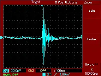
First, a lot of that ringing probably isn't actually present. The very high frequency components are making the scope show common mode bounce as differential mode signal.

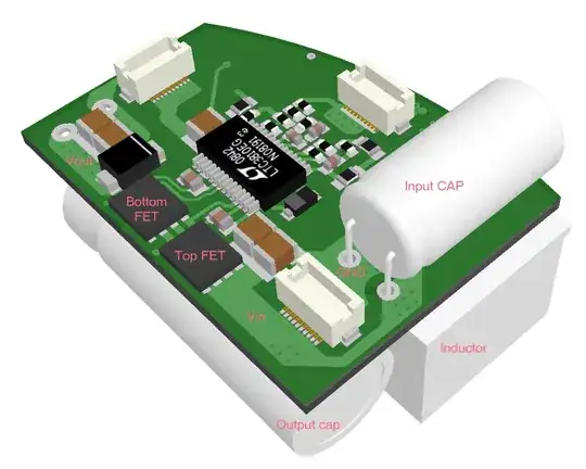
Second, all switching power supplies will have switching noise on their output. Some of this will contain high frequencies. Linear regulators may have impressive input rejection specs, but that is done with active electronics with a finite bandwidth. The new input rejection is only valid for low frequencies, like a few 10s of kHz. That is why it's standard practise to preceed a linear regulator with a ferrite bead (chip inductor) when the input voltage is coming from a switcher. The chip inductor and regulator input cap need to be physically close, the loop kept small, and the loop currents carefully considered in layout. You don't want those high frequency loop currents running accross the main ground plane.

Added:

I didn't notice that the second supply was a switcher too, but that doesn't really change anything. The high frequencies from the first switcher pulse edges are apparently making it thru the second supply whether linear or not. Try the chip inductor followed by cap straight to the ground of the second supply, not the general ground. This of course needs to be a ceramic cap, as big as reasonable for the voltage. A second smaller cap with better high frequency response might help a little too.

About common mode ground bounce. The ground is no longer a single lumped node at high frequencies, and not all at the same potential as a result. Sometimes whole sections of ground and power together can experience common mode bounce. However, what I was referring to was this common mode bounce in the scope. High frequency common mode signals can show up as differential mode signals. Dave, this was a lot of the problem in your similar question, and is likely part of the answer here too. Remember how things looked a lot better when you connected the scope probe directly to the output with a cap accross is and no place else. However in this case a downstream circuit is failing, so enough of the noise is real enough to be a problem.

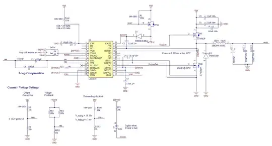
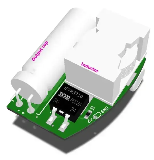
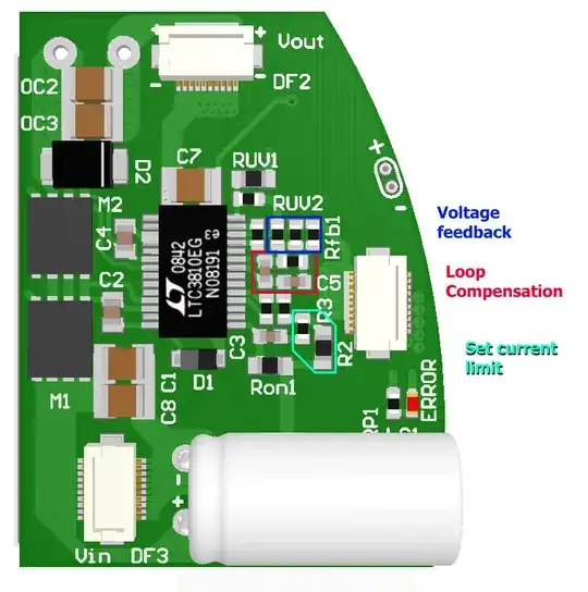
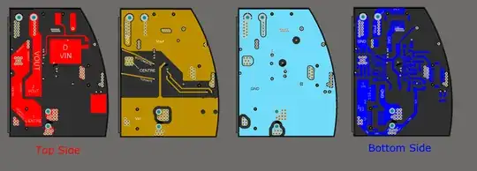
I can't tell easily from the layouts what is actually routed where. One of the important things with switchers is to contain the large and high frequency loop currents. Make sure they don't run accross the main ground plane. Each switcher should have its own ground net, and that net should be tied to the main ground in only one place. That keeps the local currents local since only the net in or out current can flow thru the single connection point.

Olin Lathrop
  • 310,974
  • 36
  • 428
  • 915
  • 1
    What is "common mode bounce" and what mechanism makes it show up as a differential mode signal in an o-scope? Is this a worthy question to pose to the community? – Dave.Mech.Eng Dec 14 '11 at 20:05
  • @Dave: We went over this in detail in your question rather similar to this one. – Olin Lathrop Dec 14 '11 at 20:28
  • Oh, sorry. I hope I didn't miss that part. I read everyone's answer thoroughly multiple times. I'll read yours again to make sure. As I recall, you identified "commom mode ground bounce" as the culprit for some of the high frequency noise as you have done here too. I guess I am looking now for its physical cause in terms of elementary principals. I am reading a book on signal integrity and I believe I now have some understanding of ground bounce. I don't get what "common mode" is referring to in this context. I haven't come across this term in the book yet. – Dave.Mech.Eng Dec 14 '11 at 20:47
  • I've added an image of the layers if it's any help. (I hope it's not too big). – Rocketmagnet Dec 14 '11 at 21:49
  • There is no linear regulator in this system. Just another DCDC 6v -> 3.3v regulator. Whatever ringing there is is clearly enough to upset the EtherCAT ASIC. Removing this power supply, and using a commercial switcher makes everything happy again, so it must be possible to reduce the ringing to the point where it's no longer a problem. – Rocketmagnet Dec 14 '11 at 21:52
  • @OlinLathrop Thanks for explaining the phenomenon further. – Dave.Mech.Eng Dec 15 '11 at 19:34
  • How can you tell whether the noise is actually there or if it's just common-mode noise? Connect both differential probes to the same point and see if it's still there? But there could be a common-mode component and a differential component. – endolith Dec 17 '11 at 21:07
  • 1
    @endolith: You can't always tell once you've taken all reasonable steps to reduce the common to differential mode coupling. Some of it is just from experience what a scope will do, especially if the probe is not grounded exactly right. – Olin Lathrop Dec 17 '11 at 22:13
7

Since PCB layout has a big influence on the performance of an SMPS, it would be great to see your PCB layout and a wider scope signal shot ( I mean increase in the horizontal axis).

It may be helpful to see the switching node's scope shot. I think this is the node you have labeled as "CENTRE". Could you probe the ground node, too?

As it happened to be the problem in this post, you may check your "Loop Compensation" part.

As you can see in this post, common mode noise and the ground wire acting as an antenna is a big deal in scoping switch-mode power supplies. Take the ground wire of the scope probe out and connect a short wire instead. You can check this answer to the post.

Edit

Your inductor selection is small in inductance for 250kHz. You will have an inductor ripple current of about 50%. Pick an inductor bigger than 13uH.

Your inductor is an overkill looking at current ratings of it. 20A Irms rating @ 20 degree celcius temperature rise is huge. I don't know your maximum and minimum input voltages, but all you need is an inductor with at least 4A Irms and 4.8A Isat. You may want to go a little higher than that but 20A is way too much.

I am telling you these by guessing that your inductor is one of SER2918H-103KL, SER2915H-103KL or SER2915L-103KL.

I can suggest you these inductors: DO5010H-153ML, DO5022P-153, MSS1278-153 or something similar.

abdullah kahraman
  • 5,930
  • 7
  • 59
  • 104
  • OK, I added the layers. I hope they help. Have to wait till tomorrow before I can add any more signal traces. I'm carefully reading through those posts you suggested. – Rocketmagnet Dec 14 '11 at 21:48
  • Could you add the silkscreen with designators on the layers? – abdullah kahraman Dec 15 '11 at 06:02
  • You should add silkscreen to the layers. Like [this](http://i.stack.imgur.com/mYtgC.png) image. I cannot still figure out from the layers where is your inductor if I omit 3D. – abdullah kahraman Dec 15 '11 at 10:49
  • The problem is that there is no room for real silk screen. Let me add one more image ... – Rocketmagnet Dec 15 '11 at 10:53
  • The inductor is on the top (red) side of the board, the LTC3810 is on the bottom (blue) side. The inductor is connected to the two pads on the red layer labelled "1 VOUT" and "2 CENTRE" – Rocketmagnet Dec 15 '11 at 11:01
  • I'm surprised you think the inductor is small. Look at the examples in the datasheet. They are all either 10uH or 4.7uH. Selecting a physically massive inductor with a low resistance and the correct inductance (according to the calculation) can't be a bad thing, surely? – Rocketmagnet Dec 15 '11 at 17:42
  • Well I said the inductance is small, yes. Check out [this link](http://www.coilcraft.com/apps/selector/selector_2.cfm). – abdullah kahraman Dec 16 '11 at 06:42
  • If you increase the current ratings of an inductor, the footprint is going to be big. Who wants that if you don't use that much current? – abdullah kahraman Dec 16 '11 at 06:45
  • Who wants that? Someone who has that space available, and wants the efficiency because it's a battery powered device. – Rocketmagnet Dec 16 '11 at 09:25
  • Okay, then stick with the same inductor package but increase the inductance and decrease ripple current so that losses will be less because the current in the inductor will be less. I would recommend SER2915L-153KL, in that series, in the same footprint. – abdullah kahraman Dec 16 '11 at 09:42
  • Let's pick MLC1565-153ML instead of SER2915L-103KL. Check http://goo.gl/4Nv5j . With the new inductor, there is a loss of 0.71 W, where it was 0.077W. Difference is 0.64 W. If before efficiency was, say, 93%, it drops down to 90.7%. You are right about that if your budget and PCB area is OK. – abdullah kahraman Dec 16 '11 at 10:08
3

Are the transients at both switching edge or only one. If one, which one.

Transients at switching edges are expected.
Managing them is the issue.
I'd guess that very careful going over the layout and seeing what flows where when is going to be what's required BUT also see below as a possibility.

Note on data sheet pages 13 & 20 they provide the option to return BGRTN (bottom FET gate ground return) to a small negative voltage to maximise shoot-through headroom. The fact that they provide this interesting feature suggests it may be needed on occasion as it is not something you'd do lightly. This should NOT be neceesary in a finished design but, by using say -2Von BGRTN now you can see if it has a major influence. (Lift IC pad and apply -2V signal. Add small cap (~~0.1 uF?) at pin to nearest ground. If it has a major effect it suggests possible shoot-through issues in the output FETs which can contribute to transients as seen.

An LC filter has got to help. Either a ferrite bead alone as Olin says, or inductor (bead or small L) plus cap or caps. IF one cap, place after the L, if 2, one eother side. . Cap grounded AT the second regulator ground point. The excessively enthused could design the filter L & C to provide an impedance that seems good BUT I'd expect that any LC whose resonant frequency was well below the frequencies in the transient (or well below smps frequency) would be liable to make a big difference.

As noted, scope grounding makes a vast difference. The late Jim Williams of LT had some good things to say about this in some app notes but much else has been written. Zero length grounding from probe near tip to ground nearest signal with no pickup loops is "good enough".
Much on this here in the utterly suberb LT AN47 - 1991 and still worthwhile.

Few would credit that this was the RIGHT way to do it :-).
It is!

enter image description here

Russell McMahon
  • 147,325
  • 18
  • 210
  • 386
  • Jim Williams died a few months ago. This app note is one of his more complex one, but he produced many others - all superb. Skimming them so you have some idea what is in them will pay dividends in times to come. Jim was one of the genuine old-school original Silicon Valley people. Very few left now. – Russell McMahon Dec 15 '11 at 11:34
  • Yes, Bob Phase and Jim Williams were the analog gurus that my age could catch only the very few moments of them. Could you tell me the names of those are left and very few? – abdullah kahraman Dec 15 '11 at 11:46