1

Theory

Schematic for Voltage Clipping with Two Series-Opposing / Bidirectional Zener Diodes

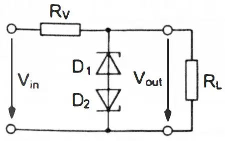
Consider the following schematic for voltage clipping with two series-opposing/bidirectional Zener Diodes \$D_{1}\$ and \$D_{2}\$:

  • The non-identical Zener Diodes \$D_{1}\$ and \$D_{2}\$ have the
    • absolute Zener voltages \$V_{Z,1}\$ and \$V_{Z,2}\$ and the
    • absolute forward voltages \$V_{F,1}\$ and \$V_{F,2}\$.
  • \$V_{in}\$ is the input alternating voltage, \$V_{out}\$ the output alternating voltage over the load resistance \$R_{L}\$.
  • \$R_{V}\$ is the dropping/series resistance.

Voltage Clipping Schematic

Voltage Plots

According to a book, this is how the voltages may look:

Voltage Clipping

Note that \$|V_{Out,Max}| \neq |V_{Out,Min}|\$, if \$D_{1} \neq D_{2}\$.

Question

What are the correct values for \$V_{Out,Max}\$ and \$V_{Out,Min}\$, if assuming \$V_{Z,1} = 20V\$, \$V_{F,1} = 0.7V\$; \$V_{Z,2} = 60V\$, \$V_{F,2} = 0.9V\$?

In this picture from this website, in accordance with these three websites and page 62 of this pdf-file, the values are given as

  • \$V_{Out,Max} = + V_{Z,1} + V_{F,2} = +20.9V\$
  • \$V_{Out,Min} = - V_{Z,2} - V_{F,1} = -60.7V\$

Are these voltages correct?

Simulations

CircuitLab

Below you can find an attempt to recreate this problem with CircuitLab.
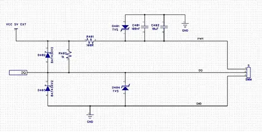
schematic

simulate this circuit – Schematic created using CircuitLab

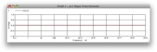
CircuitLab Simulation Result

LTSpice IV

As an addition, here are the two possibilities to realize voltage clipping with two series-opposing/bidirectional Zener Diodes, simulated with LTSpice IV:
LTSpice IV Zener Clipping Simulation

Discbrake
  • 211
  • 2
  • 11
  • The most confusing thing about your question, is that you appear to have defined voltages so that the top is more negative than the bottom... (upside down from "standard".) If that is the case then the first answer is correct. – George Herold May 16 '16 at 14:13
  • @GeorgeHerold How could V_Out,Max be lower than V_Out,Min? Does this have anything to do with the question, whether V_Z and V_F are defined as absolute values or no whter V_Z < 0 and V_F > 0? – Discbrake May 16 '16 at 14:29
  • Your question is about a change in sign... so it depends on how you define the voltages. – George Herold May 16 '16 at 14:31
  • @GeorgeHerold What if the given V_Z and V_F are all absolute values, e.g. V_Z_1 = 10V, V_F_1 = 3V; V_Z_2 = 5V, V_F_2 = 1V. What would the numeric values be for V_Out,Max and V_Out,Min ? – Discbrake May 16 '16 at 14:41
  • 1
    set the resistors to 1k, simulate, done . the PN junction resistance can be (I'm guessing) tens of ohms. – user55924 May 16 '16 at 14:46

2 Answers2

2

The simulation does work correctly. But you cannot see the clipping, because the currents are too high. Consider those Z-Diodes you selected are specified for 1.3W. So they will have a steep differential resistance. And your setup forces 10A through them.

Increase R_V and R_L to reasonable (K) values (I recommend choosing R_L >> R_V) and select your input voltage accordingly. Then your simulation will yield something visible.

Ariser
  • 3,846
  • 3
  • 23
  • 43
1

Regarding the sources you presented the correct is :

VOut,Max=+VZ,1+VF,2 (diodeZ1 is reverse biased while diodeZ2 is forward biased)

VOut,Min=−VZ,2−VF,1 (diodeZ1 is forward biased while diodeZ2 is Reverse biased)

I think in your experiment your problem lies within the zener current. R_V mightn't not be correct , how did you choose this value?

check this reference on zener diodes and this question asked before on zener current

ElectronS
  • 3,159
  • 1
  • 22
  • 47