2

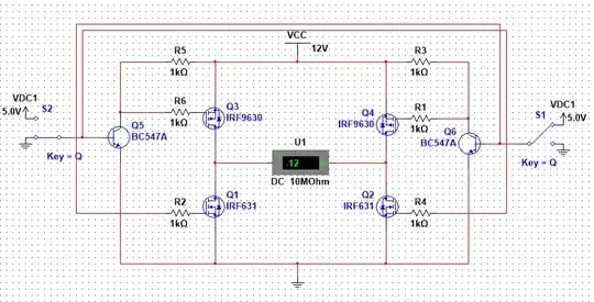
I am working on a 2WD Arduino project. Making the H-Bridge myself, and not using an IC like the L293 is a requirement for my project. After searching a while, I came across this, and based on this I made my own MOSFET based H-Bridge circuit:

enter image description here

I have some idea of how MOSFETs operate, and I can understand the working of this simpler H-Bridge:

enter image description here

However, I cannot understand how the BJTs in the first circuit work. From what I understand, when no current flows in to the base of Q5 BC547, it is in cutoff mode, and the 12V from Vcc drop across the R5 and the gate resistor R6, resulting in Vgs=0 and driving the MOSFET Q3 into cut off. On the other hand when logic is applied to the base of Q5, it goes into saturation mode. How this results in the MOSFET Q5 turning on is what I don't understand.

Also, please let me know if there are any problems with this design.

Lithiumede
  • 33
  • 4
  • 1
    Consider what would happen if the H-Bridge VCC in your simpler circuit was 12V instead of 5V. Would the P-Channel MOSFETS Q3 & Q4 ever turn off? – brhans Apr 18 '16 at 20:06
  • 3
    Note that you need some resistors in series with the bases of Q5 and Q6 in you upper circuit. You can't tie the base of a BJT directly to 5V if the emitter is tied directly to ground. – Dave Tweed Apr 18 '16 at 20:12
  • Its from the internet ,It must be good ?? – Autistic Apr 19 '16 at 03:14

2 Answers2

4

In order to turn off, a MOSFET must have a \$V_{gs}\$ which is less than some threshold. Ideally it should be 0.

For the lower transistors (the NMOS ones), this is fairly easy to understand - the source is connected to ground, so the \$V_{gs}\$ is calculated simply as equal to the voltage applied to the gate. If you have say a 5V MCU, this would be either 5V (on) or 0V (off).

For the upper transistor (the PMOS ones), it is a bit more confusing. The PMOS transistors have a \$V_{gs}\$ which is negative to be turned on. To turn on the gate must be at a lower potential than the source. To turn off, the gate must be at a potential close enough to the source to be less than a threshold.

Because the source of the PMOS is tied to 12V in the first circuit, its gate must be around 12V in order to turn off. If you drive the gate with a \$5V\$ signal directly, its gate is going to be \$V_{gs} = V_{io} - V_{sup} = 5 - 12 = -7V\$. If you drive it with a \$0V\$ signal, then \$V_{gs} = V_{io} - V_{sup} = 0 - 12 = -12V\$. If you consider that the threshold would be somewhere in the region of \$-1.5V\$, clearly the PMOS would be on in both cases - you could never turn it off.

To get around this, a level shifter must be added such that the gate is driven with either \$12V\$ (off) or \$0V\$ (on). The BJT in the circuit acts as a level shifter to convert the 5V control signal into the required 12V signal for the gate of the PMOS.

However, there is a side effect of the BJT circuit used which is that it inverts the control signal - a 0 becomes \$12V\$ (off) and a 1 becomes \$0V\$ (on). As a result the control signals have to be connected diagonally because you never want both transistors on the same half-bridge to be on at the same time - otherwise you short out the power supply.


In your latter circuit your motor supply and control signals are at the same level which means a level shifter is not needed - the 5V control signal can turn off the PMOS because it can create \$V_{gs} = V_{io} - V_{sup} = 5 - 5 = 0V\$. Because you no longer have the inverting level shifter, the MOSFETs are connected so that both transistors in the same half-bridge have the same control signal. A 0 now turns on the PMOS but turns off the NMOS, and a 1 turns on the NMOS but turns off the PMOS. This ensures both transistors in the same half-bridge never turn on at the same time.

Tom Carpenter
  • 63,168
  • 3
  • 139
  • 196
1

The BJTs act as inverters.

The difference between the two circuits is the method of control.

Your simpler circuit controls each half-bridge independently. When the p-channel FET is on, the n-channel FET is off, and visa-versa. One input controls the left half-bridge, the other input controls the right half-bridge.

The more complex circuit controls diagonal pairs of FETs. When the left p-channel FET is on, the right n-channel FET is also on. One input causes the motor to spin one way, and the other input causes the motor to spin the other way. Since the input is turning on both a p-channel and an n-channel FET, the control signal needs to be inverted for the p-channel FET, and that is what the BJT's do.

Mark
  • 2,418
  • 11
  • 14
  • 1
    That's not so the reason for having the BJTs, its a consequence of them being there. The BJTs are used to allow low voltage control signals to drive the PMOS transistors when the motor voltage is much higher (e.g. 5V MCU, 12V motor). Because the BJTs invert the signal as a result, they had to cross over the signals to avoid turning both half bridges on. – Tom Carpenter Apr 19 '16 at 07:56