20

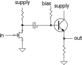
I see this circuit a lot on electret microphone preamps, but I don't quite understand it. The FET is operated as a common source amplifier, so it has gain, inverts, and has relatively high output impedance. So it would make sense to follow it by a buffer.

The BJT is common collector/emitter follower, so it would seem to be acting as just such a buffer, right? It would be non-inverting, with near unity voltage gain, and low output impedance to drive other things without being degraded. The voltage signal from the FET is passed through the capacitor to the base of the BJT, where it's then buffered and shows up at the output of the BJT.

What I don't get is why the FET's drain resistor is connected to the output of the BJT, rather than to the power supply. Is this some kind of feedback? Wouldn't it be positive feedback? (As the FET's output voltage increases, it pushes the base voltage upwards through the cap, which then pushes the output voltage upwards from the BJT, which then pulls the FET voltage upwards, and so on.)

alt text

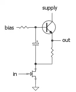
What advantage does it have over a circuit like this?

alt text

stevenvh
  • 145,145
  • 21
  • 455
  • 667
endolith
  • 28,494
  • 23
  • 117
  • 181
  • I think i can explain this, but it will take me writing a little, i will try to fill out an answer tomorrow. – Kortuk Apr 15 '10 at 05:44
  • >100 views and no answers? :/ – endolith Apr 19 '10 at 21:31
  • 2
    i think it might actually be negative feedback; as the drain voltage rises, the current into the base of the BJT increases, this increases the current from the emitter, which increases the voltage drop across the output resistor, so the voltage at the drain is driven downward, opposite to the starting assumption. – JustJeff May 01 '10 at 01:22
  • I hope to understand this question someday... we have some gifted EEs on this site... – J. Polfer May 18 '10 at 17:19
  • Here's a circuit that looks very similar, but with a JFET at the top: http://www.geofex.com/Article_Folders/modmuamp/modmuamp.htm So it's a variant of a "mu-amp", which is described on page 5 of http://www.ti.com/lit/an/snoa620/snoa620.pdf – endolith Apr 07 '14 at 20:45

6 Answers6

8

Here's the deal. The capacitor provides constant voltage at high frequencies across the BJT base-emitter + resistor combination. This causes fairly constant current through the BJT and resistor, with some high impedance Z, probably determined mostly by the BJT base resistor Rb. The FET has a high transconductance (gm = Iout / Vin), and the net gain is gm * Z. This is the voltage across the FET drain-source. The BJE emitter resistor has constant voltage across it, so there's a bias voltage added to that. The constant current allows the BJT to act as a low-impedance output buffer (=Rb/beta).

Jason S
  • 13,950
  • 3
  • 41
  • 68
  • Thanks for answering Jason, I meant to and when I saw the question today realized I forgot. – Kortuk May 18 '10 at 14:41
  • "at high frequencies" meaning "at signal frequencies"? Wouldn't constant current out of the BJT require constant current into the base? "BJE emitter resistor" should be "BJT emitter resistor"? If the BJT is just acting as a buffer, what's the benefit over a circuit like this? imgur.com/qeEZw.png The physical resistor can't be made as high as the "virtual resistance" provided by the current source? Better linearity? – endolith May 18 '10 at 15:34
  • "what's the benefit over a circuit like this": Good question. Gain looks about the same (dominated by BJT base resistor Rb... in your posted circuit it's the two bias resistors in parallel) in both cases. Output impedance looks about the same... when I first saw the circuit on this page I thought the capacitor was a battery, and I thought: "oh, of course, they're making the BJT into a constant current source, why wouldn't you just use a zener..." in which case you truly could use a constant current source w/r/t the BJT -- the advantage of this deals with parasitics in the BJT... – Jason S May 19 '10 at 01:13
  • In general, whenever you have a capacitor in series with a signal path, "low" frequency and DC signals are blocked, while "high" frequencies are passed. The capacitor creates a high-pass filter. What constitutes "high" and "low" depends on the circuit resistance and the capacitor value. – W5VO May 19 '10 at 03:00
  • @JasonS: Yeah, when I simulate this circuit, it has lower gain and worse distortion than the more straightforward one. I don't get it. – endolith May 16 '13 at 19:36
4

The current flowing through the BJT (i.e. from collector to emitter) is going to be equal to the current flowing into the base times the amplification factor of the transistor.

I_ce = beta * I_b

... if my memory serves me correctly. The FET, on the other hand, can be generally thought of as "on" (letting current flow) or "off" (preventing current flow). If the FET is "off" there will not be a path to ground for the current and no current will flow through the BJT (or conversely any current will flow to ground. The capacitor provides a path to ground (drawing current away from the base of the BJT) for "high frequency" signals. The impedence of the capacitor decreases in proportion to the product of the signal frequency and capacitance.

Z_cap = -j * omega * C
|Z_cap| = omega * C = 2 * pi * f * C

I guess that's not really much of an answer to the question, but it's what I remember from "base principles."

vicatcu
  • 22,499
  • 13
  • 79
  • 155
3

What I don't get is why the FET's drain resistor is connected to the output of the BJT, rather than to the power supply.

The resistor you refer to isn't the drain resistor in the usual sense. If the output were taken from drain, then the BJT and assorted circuitry could be considered an active load; you could replace the entire circuit "above" the FET with a small signal equivalent resistance.

If we label the base resistor \$R_B\$ and the emitter resistor \$R_E\$, the small-signal equivalent resistance seen by the drain of the FET is given by:

\$R_{td} = R_B || \frac{r_e||R_E + r_0}{1 - \alpha \frac{R_E}{r_e + R_E}} \approx R_B \$

So, for small-signals, the BJT circuit approximately "looks" like \$R_B\$ to the FET.

The really nice thing about this is that \$R_B\$ can be made quite large so that the small-signal voltage gain of the FET is large. In the 2nd circuit, the size of the drain resistor is limited by the DC operating point constraints.

For example, let's say that you have a 3V supply and a DC drain current of \$I_D = 100\mu A\$.

The drain resistor in the 2nd circuit obviously must be less than \$ 30k \Omega\$ for a positive DC drain voltage \$ V_D > 0 \$.

But in the 1st circuit, the DC current through \$R_B\$ is \$I_B = \frac{I_D}{1 + \beta} \$. So, \$R_B\$ can be much larger than \$30k \Omega\$ yielding a much larger voltage gain.

Of course, if the output were taken from the drain, we'd have a very high output impedance. But, we're taking the output from the emitter node. The voltage gain there is only slightly less than at the drain:

\$v_{out} = v_d \frac{r_o}{r_o + r_e||R_E} \approx v_d \frac{r_o}{r_o + r_e} = v_d\frac{V_A}{V_A + \alpha V_T} \approx v_d\$

Where \$V_A\$ is the Early voltage (tens to hundreds of volts) and \$V_T\$ is the thermal voltage (about \$25mV\$)

But, the resistance looking into the output node is much less than looking into the drain node:

\$r_{out} \approx r_e||R_E + R_B(1-g_mr_e||R_E) = r_e||R_E + R_B(1-\frac{\alpha R_E}{r_e + R_E})\$

So, the 1st circuit offers much higher voltage gain but somewhat higher output resistance than the 2nd circuit.

Alfred Centauri
  • 26,502
  • 1
  • 25
  • 63
2

This circuit is often called a Shunt Regulated Push-Pull (SRPP). Normally it is implemented using tubes.

In the alternative circuity the output emitter follower runs in class A and relies upon the emitter resistor for pulling down the output for a negative going signal. This can cause distortion, especially if the load has significant capacitance.

With the SRPP when the output is going negative, the FET is conducting dragging the output low through the BJT emitter resistor while the BJT is being turned off by the signal coupled through the capacitor to its base This allows the circuit to drive the output close to the ground,the BJT may even cut-off completely.

Kevin White
  • 32,097
  • 1
  • 47
  • 74
0

It is interesting. It is important that the bias resistor on the base of BJT to be high enough. If is almost the same value like drain resistor in the second diagram is no deal and in simulation you will obtain no benefit. If the bias resistor is high enough, the BJT is a voltage follower. That means in AC that the drain voltage is the same in the base of BJT and almost equal in emitter. But that means you will have no AC current on the emitter resistor, the both connections of it being at the same AC potential. Dears it is a bootstrap kind of connection that makes the drain impedance of FET very high, increasing the amplification of the system comparing with the second version. It is also interesting that the output from emitter gives low output impedance but output from drain it is the same like a transconductance amplifier, high output impedance proper for reactive charges when the current should be constant (remember recording heads of analog tape recorders).

endolith
  • 28,494
  • 23
  • 117
  • 181
0

The bipolar transistor and its emitter resistor make an active source for the jfet. This is a mu amp. The gain of the circuit is higher, yfs / yos.