3

img

I have tried hard but I don't understand how this algorithm is working.Please explain the flow chart.

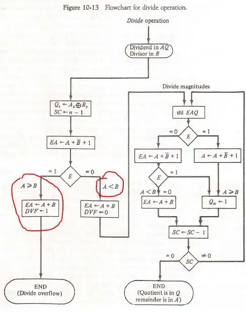
\$DVF\$ is the divide overflow flip flop.

\$A_s\$ is the sign bit of \$A\$

\$B_s\$ is the sign bit of \$B\$

\$E\$ is the register that has a carry bit

Initially the XOR operation is carried out to check if the sign bits of two numbers is equal.

The dividend is \$A\$ and \$Q\$ and the divisor in \$B\$. The sign of the result is transferred into \$Q_s\$ to be part of quotient. \$SC\$ is the sequence counter.

I am unable to understand the sequence of operations . What happens after the carry bit is checked for 1 or 0 ?

Suhail Gupta
  • 278
  • 1
  • 5
  • 14

2 Answers2

2

\$ EA \leftarrow A+{\neg B} + 1\$ is the 2-complement sum of A and B (absolute), that means that you are subtracting B from A. Then, if you have a carry bit it means that the result is negative, and |B| is bigger than |A|. Since probably the division is integer, you cannot divide a number for a bigger one and it returns an overflow, that probably should mean that the result is 0.

Otherwise, B is again summed to A (seems odd, it could save it in a register instead of subtracting and summing the same value), and then enters in a loop:

The division is calculated one bit at a time, so I think that the shift operation should be a shift right, so starting from the most significant bit of the quotient, it checks if the divisor is contained in the dividend.

clabacchio
  • 13,481
  • 4
  • 40
  • 80
2

Flowcharts are often not a very precise way of indicating what hardware is doing, since flowcharts often imply the existence of a single execution process, whereas hardware often does many overlapping and simultaneous operations.

The portions of the diagram circled in red seem a bit odd. It seems odd to latch A with the value after subtracting B, and then re-add B. More natural would simply be to not bother latching the lower part of the subtraction result. I think the flowchart might be clearer if "named values" were separated into "registers" and "values", and each step either computed values or registers. Thus, for example, one could have something like (assuming 16-bit registers)

C:T[15..0] = (A[14..0]:Q[15]) + ~B-1
if (C or A[15])
  A[15..0] = (A[14..0]:Q[15])
  Q[15..1] = Q[14..0]
  Q[0] = 1
Else
  A[15..0] = T[15..0]
  Q[15..1] = Q[14..0]
  Q[0] = 0
Endif

Every step that updates registers would represent a system clock. Events that merely compute values would not require a clock edge, but would be processed asynchronously.

Kevin Vermeer
  • 19,989
  • 8
  • 57
  • 102
supercat
  • 45,939
  • 2
  • 84
  • 143
  • I'm not really sure about your proposal: it seems to be too hardware-dependent, while this flowchart is intended as an abstract way to implement the division. But I agree that subtracting and re-adding is silly. – clabacchio Feb 02 '12 at 16:00
  • 1
    @clabacchio: Nearly all computers consist of latches interconnected by logic. In many cases, all latches are triggered by the same clock, though in some cases there are multiple clocks which fire in sequence (e.g. on the 6502, there are two clocks, so on every cycle all the latches operated by phi1 will operate, then those will hold their values while the latches operated by phi2 operate, etc.). In the software world, each step can only affect a tiny fraction of the system state, while everything else sits idle; in the hardware world, things are much more "parallel". – supercat Feb 02 '12 at 16:22
  • While I wouldn't want to suggest that an introduction to hardware division should employ every possible optimization, I would think it helpful to consider the notion of identifying which operations can happen simultaneously on a clock step. – supercat Feb 02 '12 at 16:24
  • What I mean is that a bitwise representation is quite specific, and also the pipelining can be implemented in many different ways; now I'm not so expert in divider architecture, but I know at least 3 different and many different adder and multiplier architectures. What I mean is that a step that you could see in a certain way, in an implementation is performed in a different (and often much less intuitive) way. – clabacchio Feb 02 '12 at 16:26
  • The only things I'm really doing differently, 'bitwise', are combining the shift with the next addition (perhaps a slight over-complication from a teaching standpoint, but one which will massively increase speed) and being more explicit in my notation (e.g. instead of saying EA=whatever, say "E:A[15..0] = whatever"). In some contexts, XY means (X 'and' Y), and in others it might mean a register called XY. Using a punctuation mark to indicate stacking seems like a good idea. – supercat Feb 02 '12 at 16:33
  • What I mean is that you were suggesting to divide the operations in clock cycles, that in principle is correct, but you can know before how the architecture will split the operations. With 'bitwise' I was meaning that you are implying (?) the use of 16 bit variables, just that. – clabacchio Feb 02 '12 at 16:59
  • @clabacchio: Hardware will subdivide operations into clock cycles via whatever means the designer wants; part of producing a design is figuring out what things should happen on which clock edge. In software, the time taken by individual steps is, generally, only a concern insofar as programs that run too slowly are annoying. In hardware, given that certain things happen at certain times (e.g. a clock pulse arrives every 100ns), one must arrange for other things to happen in response, within certain time windows. Subdividing into "clock cycles" is a useful simplification; everything... – supercat Feb 02 '12 at 17:12
  • ...is assumed to be in a stable state when a clock cycle arrives, and then change as quickly as possible into another stable state before the next one arrives. At 10MHz, the allowable window might be "anywhere from 0-95ns after each clock edge". – supercat Feb 02 '12 at 17:14
  • I completely agree with you about the timing and the pipelining, in which propagation, setup and hold times are fundamental; and I have been teached also the importance of throughput. My observation was just that at the algorithm level, such as in this question, these aspects are impossible to determine, because the algorithm is architecture-independent, and each implementation differs from the other, still performing the same operation. – clabacchio Feb 02 '12 at 17:26
  • @clabacchio: I guess I tend to think of the subdivision of work as being an essential part of what a hardware algorithm *is*. While it's certainly possible to have many nearly-identical variations of an algorithm which subdivide operations slightly differently, that's true in software as well. What matters in hardware is, in some sense, how many times a given signal will have to loop through the same circuitry; it is that looping, after all, which creates the need for clocked registers. – supercat Feb 02 '12 at 17:48
  • [this](http://writphotec.com/mano4/Supplements/Mulitpliers_Dividers_supp4.pdf) is what I mean as "hardware implementation" versus flowchart representation; as you can see, is quite detailed (at block level) – clabacchio Feb 03 '12 at 08:18