1

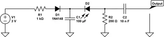
I got a circuit for a photodiode, but unfortunately without datasheet and explanation. Now I am a bit confused what the purpose of the different parts is:

schematic

simulate this circuit – Schematic created using CircuitLab

As far as I understood, the resistor R1 and the diode D1 are providing a voltage drop, while the capacitor C1 provides a voltage buffer. R2 is doing ?, and C2 is coupling out DC current. Is that correct? And what is the purpose of R2?

arc_lupus
  • 724
  • 1
  • 8
  • 28

1 Answers1

2

The photodiode has some parasitic capacitance. Its time constant is hence C times the load resistance. R2 plays the role of this load here; a sufficiently small value such that the response time will be acceptable for whatever application this circuit is intended. It also converts the output current into a voltage, thus giving the circuit a definite gain (200 V/A) independent of the load (within reason).

C2 also needs not to be fully charged if it is to work as a coupling capacitor, and R2 allows for that to happen by providing a d.c. path to ground.

Oleksandr R.
  • 1,644
  • 11
  • 14