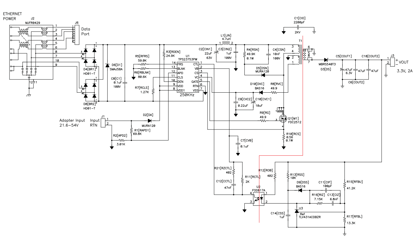
I often see this in practical SMPS designs. An optocoupler & voltage reference pair is used for informing the controller section about the output voltage level. However, when I read the datasheet of the optocoupler in the circuit, I see that the given signal characteristics "rise time" and "fall time" are higher than the switching period of the controller circuit.
Example
See this circuit in this article.

In the schematics, it says that the switching frequency of this circuit is 250kHz, which means the switching period is 4us. In the optocoupler datasheet, the rise time is given as 4us (typical) and 18us (maximum). The fall time is 3us (typical) and 18us (maximum). The signal has to rise and then fall, so it takes typically 7us (36us at maximum) for a pulse. An engineer must make his design considering the worst case circumstances, so we should take the maximum pulse time as 36us, which is 9 times the switching period.
Wouldn't it mean that the controller will respond to an output change 9 periods late? Is this much latency acceptable, doesn't it cause output voltage level controlling problems? Or, is there anything I'm missing here? Can you please explain me how does this kind of SMPS designs work with all these slow optocouplers?