4

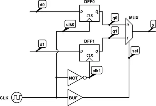
Consider the following circuit, which multiplexes the d0 and d1 inputs to the y output in one clock cycle (i.e., double data rate, DDR).

schematic

simulate this circuit – Schematic created using CircuitLab

Which may be the result of synthesizing the following Verilog code:

module ddr_mux (
    input wire clk,
    input wire d0, d1,
    output wire y
);

reg q0, q1;

always @(posedge clk) q0 <= d0;
always @(negedge clk) q1 <= d1;

assign y = clk ? q1 : q0;

endmodule

I have the following timing requirements:

  • q0 must not change while the MUX select input is at 0
  • q1 must not change while the MUX select input is at 1

In other words,

  • y must have at most two transitions per clock period.

If the synthesis and timing analysis tools do not know these requirements on the y output, they have the freedom to implement the circuit with an arbitrary timing relationship between q0, q1, and sel. Here is an example of how this could go wrong:

DDR Mux counterexample

And here is the desired behaviour:

DDR Mux desired behaviour

How do I correctly express this in the form of SDC constraints to be read by Cadence synthesis and timing analysis tools?

mkrieger1
  • 143
  • 7
  • I'm not familiar with verilog, so I'm not posting this as an answer...However, I'm working on a frame-timing circuit where I solved the same problem using ans AND gate + SR flip-flop on each Q input line. Use d0 AND CLK for Set on q0 & d1 AND NOT CLK for Set on q1; then use NOT CLK Reset q0 & CLK Reset q1 – Robherc KV5ROB Mar 03 '16 at 15:31
  • Thanks for your input. But isn't what you describe just accomplished by using D flip-flops as shown in my drawing? – mkrieger1 Mar 03 '16 at 17:20
  • If your D-flipflops (sorry, didn't catch the DFF labels) are latching based on CLK state, then where is your problem/question? I assumed, based on your statement of needing to ensure no more than 2 Y transitions/clk that you were seeing a failure there. – Robherc KV5ROB Mar 03 '16 at 21:30
  • @RobhercKV5ROB: I've updated the question to illustrate what the problem is. – mkrieger1 Mar 04 '16 at 10:31
  • Ok, looking at your added information, I think you're trying to describe a problem due to mis-matched propagation delays between your DFFs and your MUX selector. In practice, so long as the mis-match is small enough, it is often negated by output/load parasitics. If you're 'seeing' a problem with it in your (actual) output, you may need to add (a) buffer gate(s) to the circuit to delay whichever component(s) is(are) 'getting ahead.' – Robherc KV5ROB Mar 04 '16 at 15:49
  • @RobhercKV5ROB: Exactly. And I want to specify the rules which make the mismatch illegal. – mkrieger1 Mar 04 '16 at 15:51
  • sorry, I wish I could help more, but I'm unfamiliar with the software tool you are using :( – Robherc KV5ROB Mar 04 '16 at 15:53

0 Answers0