0

Given an AND gate, an OR gate, and inverters as needed, design an SR flip flop with S and R active low (0).

I understand that to make such a flip flop, I would have to place inverters on the circuit so that the AND and OR gates behave like NOR gates, as NAND with S=0, R=0 would lead to a race condition. However, I have no idea how I would place inverters in such a way for it to behave like NOR gates.
Null
  • 7,448
  • 17
  • 36
  • 48

1 Answers1

0

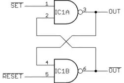
You have a bunch of questions jumbled together, and we're not going to do your homework for you anyway. However, consider this very basic flip-flop circuit:

Look at this carefully and understand how it works. You should then be able to figure things out from there.

Olin Lathrop
  • 310,974
  • 36
  • 428
  • 915
  • That looks like a latch not a flip flop. – jbord39 Aug 09 '16 at 22:31
  • @jbord: The distinction is usually that a flip-flop works on the edge of the clock signal, and a latch on the level of the clock signal. This is a very basic circuit that doesn't have a clock, and can be used as the memory element of both a latch and a flip-flop. You could probably call this circuit either without really being wrong, but the latch/flip-flop distinction is neither useful nor meaningful at this basic level. That distinction is more about what you put in front of the inputs of this circuit. – Olin Lathrop Aug 12 '16 at 17:39
  • I am familiar with the differences. What you posted is a latch. You can call it a flip flop all you want, that does not make it so. And the distinction between flip flops and latches are most meaningful at the basic circuit level, which is where their nuances can be understood (different setup and hold time in a flop and latch, for example). A flip flop is two back to back latches with opposite polarity clock, creating a lock and dam system (edge triggered). Google latch based or flop based VLSI design to see the differences. – jbord39 Aug 12 '16 at 17:46
  • http://www.eetimes.com/document.asp?doc_id=1278980 A link from EE times. Notice distinction between latch and flip flop. – jbord39 Aug 12 '16 at 17:49
  • @Jbord: I read the latches versus flip-flop section, and it supports exactly what I said about edge versus level of the clock signal. Again, the circuit above doesn't have a clock input. – Olin Lathrop Aug 13 '16 at 01:12
  • This is an SR latch without an enable, which is transparent 100% of the time. Adding a clock enable, it is still a latch. Put two back to back with inverted clocks (enables), and you have a flip flop. – jbord39 Aug 13 '16 at 01:40
  • As it says, you cannot time borrow with a normal flip flop. Clearly the "latch" you showed allows time borrowing: it is transparent (level sensitive) the entire cycle. Only by putting two back to back with opposite phase clocks do you create an 'edge triggered' (edge meaning clock or enable edge). – jbord39 Aug 13 '16 at 01:43
  • @jbord: This is getting deep into meaningless details. – Olin Lathrop Aug 14 '16 at 02:29
  • If you say so... Just stay away from designing my CPU!! – jbord39 Aug 14 '16 at 03:08