5

I am reading about microcontrollers now and i ve been confused.

I am reading some pdfs and there is a symbolism of tristate condition High->High/Low. Meaning going from High to high and low at the same time. How can this be possible?? what is the meaning behind this??

It has also some process of going from tristate to high and low at the same time and the opposite.

Its also shown in some waveforms after.

Brian Carlton
  • 13,252
  • 5
  • 43
  • 64
Nick Alexis
  • 55
  • 1
  • 4
  • 4
    It would help if you could refer us to a copy of the PDFs concerened or provide a scanned image. This will be a matter of interpretation and if we can see what is being said we should have no trouble explaining it. – Russell McMahon Oct 25 '11 at 18:35
  • http://alexander.ee.auth.gr:8083/eTHMMY/archive/147/customStore/hardware0.pdf Thats the pdf i am talkin about last pages. I thing What Mr Lathrop said is right thats what i thought too. – Nick Alexis Oct 25 '11 at 21:39

8 Answers8

14

Any signal can only be at one voltage at one time in any one place. Digital microcontroller pins can be actively pulling high, actively pulling low, or not pulling any particular way, meaning they are high impedance and the line is supposed to be driven by something else. There is no such thing as going to "high and low".

What you are probably confused by are timing diagrams. These show a line high when at the logic high voltage, low when at the logic low voltage, and often in the middle when the pin in question is not driving (high impedance, sometimes also called "tri-state"). In some conditions shown by the timing diagram, it is known that the pin will be actively driving, but the data value is not know or is irrelevant to the description. In such cases, lines often drawn both at the high and low levels to show the pin could be either. Of course it can only be one of those in any one real instance, but when the timing is independent of the data value this is what it usually done. After all, it would be misleading to show the line just low or just high. That would indicate that the pin had to be specifically low or high in that case, not that it can take on a arbitrary data value at that point in the logic.

Olin Lathrop
  • 310,974
  • 36
  • 428
  • 915
3

Tristate means the pin can be in three states: 1, 0 or high impedance (Hi-Z)

I am not sure exactly what you read (link to the pdf would be useful) but it does not mean the pin can be high and low at the same time. I suspect the "waveform" may have been a timing diagram in which e.g. data signals may be represented by high and low (as there is no way of knowing which they might be at that point)

An example - in a PIC microcontroller, you have a TRIS (tristate) register, which sets the pins from output (low impedance) to input (high impedance)

Oli Glaser
  • 54,990
  • 3
  • 76
  • 147
1

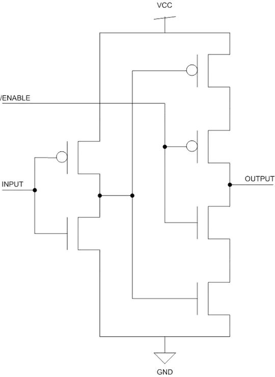
Voltages (signals) are never both high and low at the same time. They can however be "undefined" or "floating" or "tri-state" or whatever term you like. This state is usually called high impedence. A (not the only) way of achieving this state in CMOS logic is an inverter followed by an inverting latch. One signal to the block is an /ENABLE signal and the other is INPUT. This bit of logic can be used to multiplex a shared bus among many potential senders, as one example.

enter image description here

If /ENABLE= 0 = GND then OUTPUT = INPUT. If /Enable = 1 = VCC then OUTPUT = High Impedence (i.e. floating). That is to say, when /ENABLE = 1, the OUTPUT is effectively disconnected from either rail (e.g. VCC or GND) because the inner PMOS and NMOS transistors are "off." Besides that caveat, what I've drawn is just two cascaded inverters.

As a note, the / before the ENABLE signal name is meant to reinforce the notion that the signal is inverted logic. You can read that signal name (/ENABLE) as "Not Enable."

vicatcu
  • 22,499
  • 13
  • 79
  • 155
  • I think you need another inverter somewhere -- either between the enable line and the pFET it's currently connected to, or between the enable line and the nFET it's currently connected to. – davidcary Oct 26 '11 at 03:43
0

A tri-stated signal is neither low nor high. It can be thought of as 'disconnected' from the rest of the circuit.

V = IZ, if Z = some big number:: V/{BIG NUMBER} = very small amount of current flowing.

(Z being impedance - which is "complex resistance". This is why tri-stated is sometimes called Hi-Z)

dext0rb
  • 3,681
  • 2
  • 28
  • 41
0

It would help if you could refer us to a copy of the PDFs concerened or provide a scanned image. This will be a matter of interpretation and if we can see what is being said we should have no trouble explaining it.

The following lists all the valid output pin types and states that come to mind. (E&OE). Your descriptions will be describing a transition between some of these tates. The pullable Schmitt trigger output and quasi output types sound possible candidates.

Possible output pin states.

Active high/low. Pin is in only one of these at a time but is driven to one or other state. Intermediate state is transited rapidly and is not considered a valid condition and characteristics in transition state are usually not defined.

Open drain or open collector. The driver can connect the pin low or can let the pin float. There is no active high drive. The pin is pulled high when in an undriven state by an external resistor or load to high or possibly by an internal resistor - if so it is probably switchable as an option. Open drain is usually actively pulled to ground but a high side referenced pin would be equally valid with pull down load or resistors. Open drain is a means of allowing 2 or more pins to drive the same circuit simultaneously. More than one pin can legally drive the connection at the same time BUT any active low will pull the connection low so it acts like a multiple input AND gate
ie Output = A and B and C and ... .
Any low means the output is low.
All high means the output floats and would usually be pulled up.

Tri-State. The pin has either high and low drivers or a low side open drain driver but these can be all disable leaving the pin in an uncommitted state.
This is known as tristating (high, low, open).
It is expected that the pin would be pulled to a legal high or low level by some other pin connected to the same connection.
Tristate mode allows 2 or more pins to drive the same line at different times.
Not more than one can legally drive the line simultaneously.

Quasi output. Some manufacturers provide a pin with as purposefully very weak drive so that it can be overridden by a srong input signal if desired.

Schmitt trigger self latching. This is different than a Schmitt trigger input and similar to the quasi output above.
A non inverting Schmitt trigger input gate has a weak pull up/down connected from its output back to the pin. Thus it senses its own state and will self latch either high or low. If this weak pull up/down is overridden by a strong input sighnal the pin will follow the signal and will remain in the last state when the input signal is removed (ie when the driving source goes high impedance.)

Input:

Input pins are high impedance pins with internal logic monitoring the level of the pin. An optional internal pullup may be provided. An optional internal pull down may be provided but this is less common. Pullups (or downs) are usually "weak" comoared to typical exteral drives and may usually be easily overridden by internal signals.
An input pin may have an internal inwards pointing Schmitt trigger such that the perceived state of the pin flips suddenly when the Schmitt level is transited. This tends not to affect the state of the actual pin signal so is different than the Schmitt trigger "pullable output" mentioned above.

Russell McMahon
  • 147,325
  • 18
  • 210
  • 386
0

To amplify Mr. Lathrop's answer: timing diagrams have two aspects: (1) what a device will do, and (2) what a device will expect from other devices. Timing diagrams almost always combine some of both (since most devices exist for the purpose of causing some response to external signals). In many cases, some signals on the timing diagram will show what's assumed on the input, and others will show what's assumed on the output; sometimes bidirectional signals may combine both. My preference for timing diagrams involving bidirectional signals is usually to have input and output functions shown on different lines; when they're on one line, it's sometimes easy to tell what's input and what's output, but sometimes it can be confusing.

With regard to device inputs, there are a few "symbols" to be aware of. A line which is solidly high means the input is assumed to be high. Likewise one which is solidly low. A line which sits in the middle or one which is cross-hatched high and low means that the device won't care what the input does at that point; it could sit high, sit low, or bounce arbitrarily between high and low. If the line starts high and then goes low with a bunch of parallel diagonal lines, that means the device will expect the input to go from high to low exactly once, but won't care precisely when it happens. Likewise if the line starts low and goes high. If there are parallel horizontal lines at high and low, that means that the signal may legitimately be high, or it may legitimately be low, but must remain in its present state for the duration of the indicated part of the diagram.

With regard to device outputs, the "symbols" are mostly similar, except that they either indicate what the device can be expected to do or indicate when the device can't be expected to do anything in particular. The one major difference is that a line centered between high and low does not mean unspecified behavior--it means that the device is guaranteed not to output a strong high or a strong low (the device may output very weakly high or low, but not so strongly that any other device would have difficulty whatsoever overpowering it).

An important thing to note with timing diagrams, by the way, is that they are generally not drawn to any particular horizontal scale. Certain moments in time will be labeled, with labeled arrows connecting them. Generally, the function of a timing diagram is to make statements like the following:

  1. For correct operation, event X must happen at least time t before event Y
  2. For correct operation, event X must happen within time t of event Y
  3. For correct operation, event X must happen between time t1 and t2 of event Y
  4. For correct operation, event X must NOT happen between time t1 and t2 of event Y
  5. If event X happens, device will output event Y within time t
  6. If event X happens, device will output event Y no sooner than time t
  7. If event X happens, device will output event Y between time t1 and t2 afterward.

An important thing to realize is that the statements made by a timing diagram are often independent. If signals are not marked as having any particular timing relationship relative to each other, their relative placement on the diagram should be regarded as coincidental. For example, the timing diagram for a ROM chip might show /CS going low, and then /OE going low, and have an arrow from the falling edge of /CS to the output with a labeled time of 100ns, and an arrow from the falling edge of /OE to the output with a labeled time of 50ns. Such a diagram does not mean the falling edge of /OE must occur before the edge of /CS. It means that the state of the output is not guaranteed except when /CS has been low for at least 100ns and /OE has been low for at least 50ns. Unless explicit timing relationships are stated between /CS and /OE, they may go up and down arbitrarily, with the sole caveat being that unless they have been low for the required durations there's no guarantee as to what the chip will output.
supercat
  • 45,939
  • 2
  • 84
  • 143
0

For tristate we have high, low, and high Z where Z is impedance. A tristate device is often used in communications. If you attempt to connect three bistate (high or low) device on to a common bus. One is inactive, one is sending and one is receiving. The first device going to it's low state, pulls down the line for the other two so they cannot send data. With tristate, the devices can go to the high Z mode instead of low, now the remaining tow device can send data normally.

Jim C
  • 1,997
  • 12
  • 11
0

I don't think that it has been explicitly mentioned yet in these answers that a timing diagram may show a line in both states to indicate that it is carrying data that cannot be known until the device is working, so the line could be either high or low when it is in use, and is symbolically shown as both at the same time.

Harry Weston
  • 2,170
  • 3
  • 24
  • 28