4

So this is a question that was asked in one of the exams. As you know, there are 2 ways to get the boolean expression for the sum of the full adder.

Given X and Y are inputs, C0 is the carry from previous adder and C1 is the carry output and S as the sum, described as:

C1 = X.Y + C0(X + Y)

C1 = X.Y + C0( X ^ Y )

is the other expression with an XOR gate (^)

so which expression is better in building the Full Adder? Should we use the XOR or OR and what is the reason for the selection?

EDIT: I previously mentioned it as sum which is a mistake, it's for the carryout.

Thank You
b degnan
  • 3,167
  • 2
  • 17
  • 36
ManZzup
  • 141
  • 4
  • 1
    This looks like homework / coursework with no attempt to solve. A quick google search shows numerous answers to this query. – Peter Smith Jan 17 '16 at 16:36
  • @PeterSmith believe me i did countless amount of googling, but there's no definitive answer explaining why XOR is better than AND. i need at least a circuit wise prove through the TTL or CMOS implementation of the gates to make sure which to chose and i cant come up with that by my own :/ – ManZzup Jan 17 '16 at 16:39
  • Aside from the fact that neither of those two expressions is correct as written... they are both expressions for carry out not sum. The thing to remember is that both Sum and Carry are built into the same circuit - so think about both together and which requires fewer gates. – Tom Carpenter Jan 17 '16 at 17:07
  • *but there's no definitive answer explaining why XOR is better than AND* <-- that's the point. – Marcus Müller Jan 17 '16 at 17:25
  • I'm really sorry for the errors in the question, im pretty screwed after 3 weeks of exams :/ – ManZzup Jan 17 '16 at 17:26
  • @MarcusMüller but the issue is they are asking for an advantage at least. may be in the implementation or propagation time – ManZzup Jan 17 '16 at 17:27
  • Some technologies can do OR gates more easily, other NAND, other AND... It all depends on what you're using to build your stuff. – Marcus Müller Jan 17 '16 at 17:28
  • @MarcusMüller still any special consideration in building a full adder? I'm convinced there's a specific reason given that it is given as fully formed question – ManZzup Jan 17 '16 at 17:37
  • I'm convinced there's more to the picture, then :) – Marcus Müller Jan 17 '16 at 17:41

2 Answers2

12

If I were doing a silicon implementation, I would use an XOR because of the symmetric properties. Symmetric circuits use much less power because the stack size is the same that does a few useful things:

  1. Greater effective serial resistance when "off" due to the "stack of 2",
  2. Better matched channels because DIBL is the same on pull up and pull down networks,
  3. More uniform switching time because charge sharing is similar (very dependent on #2),
  4. Usually, better devices as far as lithography so better threshold matching.

A very complete discussions exist for "mirror adders" if you look out there, but they probably only mention #1 and #2.

If you have it in a package, none of this matters.

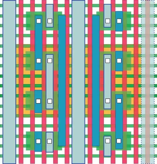
One thing that will not be in the discussions will be that at smaller feature sizes, we try to do everything as symmetric as possible because of metal rules and coloring. Below is an export image of an XOR from a commercially available FinFET process at 14nm that illustrates the metal coloring. The blue/lighblue are different lithography steps.

XOR layout image

kelalaka
  • 145
  • 7
b degnan
  • 3,167
  • 2
  • 17
  • 36
  • Using XOR requires 2 times more transistors than using (N)OR ... – Paebbels Jan 17 '16 at 22:22
  • 3
    It does, but that does not mean you can clock it faster or have better static performance. The dynamic power will be lower with the NOR in theory, but in practice you will find that the ripple skew causes the transitions to not be as sharp. 0th order, you are correct, but I wouldn't build a system that way if I wanted good power/variance performance. – b degnan Jan 18 '16 at 01:13
  • Thank you @bdegnan i will check if this is the answer they will give :) – ManZzup Jan 18 '16 at 22:41
  • 1
    Can you explain what does metal coloring mean? Yes, there are two steps due to process ~~limitations~~ ahem requirements I assume, but is that all there's to it? And if so, why on Earth would someone call it *coloring* rather than *interleaving* (since that's visually what it is)? :) – Kuba hasn't forgotten Monica Jun 29 '20 at 16:42
  • @ReinstateMonica Due to the lithographic limitations, you can have two metals on the same layer, but you need to go to a higher metal layer to connect them. I have no idea why the term "color" is used, but it's probably due to the fact that VLSI tools use color to determine GDS layers. I've been updating this recently: https://crypto.stackexchange.com/questions/81191/why-do-5g-4g-etc-use-non-conventional-algorithms/81193#81193 There's links that are pertinent to layout. – b degnan Jun 29 '20 at 16:57
0

Using an XOR requires 2 times more transistors.

XOR => 4 T
OR => 2+1 T (NOR + NOT)

If you invert your carrychain after each fulladder, you can spare the NOT gate and use an NOR gate -> 2 transistors.

There is also a 3 T XOR gate using a transfer gate, but this reqires signal refreshing after N stages.

It's common to measure CMOS logic in transistor pairs: 1 T = 1×PMOS + 1×NMOS transistor

Paebbels
  • 3,897
  • 2
  • 18
  • 43