For NAND, I am doing a truth table for it and then truth tables for all the possible combinations, but as you can see the process is very long and I am still yet to get an answer. Same goes for NOR gate. How do you go about it?
Asked
Active
Viewed 7.8k times
3 Answers
7
An alternate approach is given.
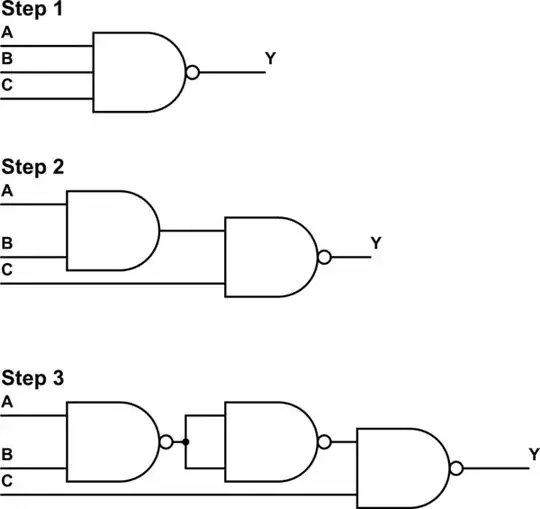
simulate this circuit – Schematic created using CircuitLab
The schematic represents the function: $$Y = \overline{ABC} = \overline{\overline{\overline{AB}} C}$$
nidhin
- 8,197
- 3
- 28
- 46
-
How did you find Step 2 from Step 1? – studious Jan 18 '16 at 14:02
-
@studious \$Y=\mathtt{nand(A,B,C)} = \mathtt{not\{and(A,B,C)\} = \\ not\{and(and(A,B),C)\}=nand\{and(A,B),C\}}\$ – nidhin Jan 18 '16 at 16:34
5
As equations.
\$\overline{ABC} = \overline{(AB)C} = \overline{\overline{\bar A+\bar B}\cdot C}\$
Ignacio Vazquez-Abrams
- 48,282
- 4
- 73
- 102
-
-
1It's also something that [should have been covered in Boolean Algebra 101](https://en.wikipedia.org/wiki/De_Morgan's_laws). – Ignacio Vazquez-Abrams Jan 16 '16 at 21:59
-
-
1Though to build that from NAND/NOR gates would take four gates in total. It can be done with just three gates. Notice that the \$(AB)\$ is a 2-input AND gate, which is equivalent to \$\overline{\overline{AB}}\$ which is a 2-in NAND gate followed by an inverter (another 2-in NAND with both inputs tied together). So \$\overline{ABC} = \overline{\overline{\overline{A \cdot B}}\cdot C}\$ – Tom Carpenter Jan 17 '16 at 03:53
-
2
Note that in the above answers, there are three propagation delays for A and B, but only one for C. Therefore, if propagation delays matter, put two nand gates in series in line C, wired as inverters.
richard1941
- 632
- 3
- 7