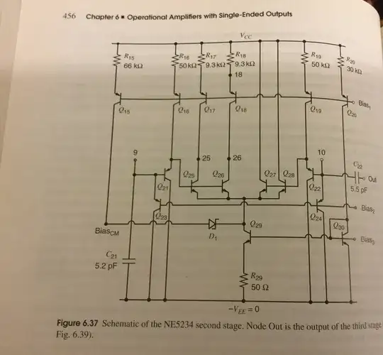
I had a question in mind. I was reading "Design and Analysis of Integrated Circuits" by Gray and Meyer... In the edition 5 there is an analysis of a Low power OpAmp NE5234... In the second stage of Amplification an unbalanced differential pair is used. I wanted to know why is that? Although it might not have any effect on voltage gain but it might introduce some other voltage offsets... Designer could've used a symmetrical structure, why it hasn't been done so? Thanks in advance...
-
Have you read this: https://www.google.com/url?sa=i&rct=j&q=&esrc=s&source=images&cd=&ved=0ahUKEwiq7b66k9TJAhUBmhQKHX0KBIoQjRwIBQ&url=http%3A%2F%2Fwww.eda.ei.tum.de%2Ffileadmin%2Ftueieda%2Fwww%2FMSCE%2FATIC%2F07.07.2010%2FBJT_OPAMPs_update.pdf&psig=AFQjCNFujlbmZjVfwKYlnm8by_XkK_sjww&ust=1449934949855812&cad=rja - it contains an extensive analysis of the chip. – Andy aka Dec 11 '15 at 15:48
-
I've gone over that document, does not specify a reason for \$ Q_{25-26} \$ seeing current source loads whereas \$ Q_{27-28} \$ is directly connected to the supply. – deadude Dec 11 '15 at 16:26
-
@Andy aka, Thanks for the answer, but those particular slides are summarized sentences from my book! In the book it is not explained... – Miad75 Dec 11 '15 at 16:26
-
@MiadLaghaei, could you please tell me what 9,10, 25, and 26 refer to? – Dave Dec 22 '15 at 23:08
-
@Dave, 9 and 10 are differential output from the first stage of amplification, 25 and 26are the outputs for this stage... – Miad75 Dec 24 '15 at 18:10
2 Answers
A differential stage has the advantage of cancelling out even order harmonics. However, they were using only one polarity of it's output and didn't need to waste transistors as loads for one half of the differential. I'm not 100% sure, because I didn't design this. This is just my best guess.
- 1,792
- 8
- 17
Well thanks all for the answers, But I found the answer myself but I just remembered to post it ;) ...by using unbalanced differential pair it ensures we don't have any floating node (as in differential stage with 2 active loads (NOT CURRENT MIRROR))... There are 2 scenarios possible: 1. If the designer wanted to use 2 current sources then he MUST've used common mode feedback to ensure no floating points exist...then it would've had it's own problems... 2. If he wanted to use a mirror, it would introduce a Mirror-Pole which would deteriorate phase margin...
- 37
- 6
