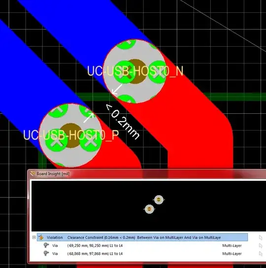
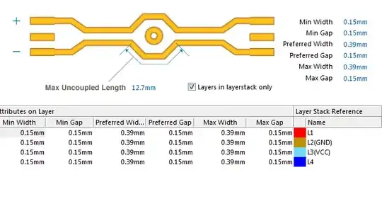
In Altium 14.3 how can one define via to via clearance in differential pair routing to produce a different spacing between via to via and track to track?
I defined a design Rule: Electrical->Clearance->ClearenceViaToVia[IsVia,IsVia] to 0.2mm
Because my differential pair routing rule is set to MaxGap 0.15mm Altium violates it in interactive routing mode, which is pretty annoying


