6

We have some controlled impedance traces on layer 4 of a board. Layer 3 is a GND plane. Layer 5 is a 3.3V plane. Both planes are unbroken (they occupy the entire layer), with the exception of vias and holes.

There are a lot of holes on this PCB, because we have a lot of through-hole connectors. See the not-so-pretty picture below:

traces going through holes

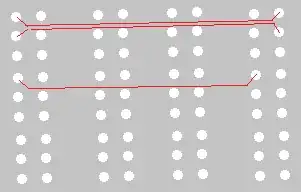
The white circles are the holes in the PCB. My question is, how do all these holes affect the impedance of the traces? Is there a minimum distance that should be maintained from the holes to ensure that the impedance is within specified tolerances (100ohms +- %5-10 for differential lines for example)

Another somewhat similar question: Consider the picture below:

traces above respective planes

Let's assume that layer 3, the GND plane layer is now split into 2, one AGND and one DGND section. Do the traces running entirely on a single plane layer (like in the picture) maintain the controlled impedance value? Is there a limit to how close they can get to the edges of the planes before starting to show deviations from the target characteristic impedance?

SomethingBetter
  • 2,260
  • 7
  • 26
  • 33
  • I do not have the time to give this the answer it deserves, but I will say one thing. Do not run traces between different ground planes. This is BAD. – Kortuk Sep 24 '11 at 21:18
  • Between ground planes? Yes we do not do that. But wondering how the two situations described above affects characteristic impedance. – SomethingBetter Sep 25 '11 at 08:06
  • @Kortuk: As I said, we are *NOT* passing over ground planes. I'd appreciate if you comment on the other two situations described above instead of worrying that I'll pass over the two planes :) (The effect of through-hole pads, and the effect of plane splits in the case that I am not crossing over them) – SomethingBetter Sep 25 '11 at 08:36
  • 1
    "yes we do not do that." I missed the not. No worries, the comment was added for the public on the whole though as others can learn also. I have to find my copy of high speed digital design to give you an explicit answer and I just recently moved. – Kortuk Sep 25 '11 at 09:27
  • 1
    As Kortuk says, [High Speed Digital Design](http://www.amazon.com/High-Speed-Digital-Design-Handbook/dp/0133957241) would probably help out here. – Tom Davies Oct 20 '11 at 10:52
  • @SomethingBetter, I spent some time with it, I have some ideas for what affect it would have but I really need to make some computational models to tell you any more then others already have told you. – Kortuk Jan 07 '12 at 14:28

3 Answers3

4

Trace characteristic impedance, that of either microstrips or stripline, is determined taking into account the PCB stackup/geometry without vias. At 3x the calculated required trace width nearly all (e-3) of the original signal will have dissipated.

The signal return path is important for high-speed currents. At high frequencies current follows the path of least inductance, not least resistance, which is normally whichever path is closest to the signal trace. Return current density falls off inversely with 1+(D/H)2, at a point D units away from the signal trace on a return layer H units thick[1].

So, one needs to pay attention to the D/H ratio in addition to trace width W: stay 3xW and 4xH away from the trace (4.36xH.. for 95% dissipation).

[1] See eq. 5.1, pg. 190, of High-Speed Digital Design by H. Johnson, M. Graham.

tyblu
  • 8,167
  • 6
  • 40
  • 70
3

For the first question, I would analyze the board in HyperLynx or similar post-route signal integrity tool. If I didn't have such a tool, I would keep the space to hole spacing at 20 mils or 4x the trace width, whichever is more.

Brian Carlton
  • 13,252
  • 5
  • 43
  • 64
2

If the height between the signal trace and the ground plane is h, a fair rule of thumb is to keep all potential perturbing features at least 3h away from your traces. If you can manage more separation, that's even better.

Also, if the trace length is less than 1/10 wavelength at your frequencies of interest, determined by the rise and fall times of your digital signals, remember that it probably doesn't matter much what you do. That's a trace length of 1.4 meters at 10 MHz or 14 cm at 100 MHz. If your sketch is showing through holes spaced at 0.1 inches, it looks like your board is less than 1 inch square and you could get away with well over 100 MHz signals without worrying excessively about controlled impedance and careful terminations.

Edit

This is not to say you should totally ignore good design practice and get rid of your ground plane or run traces across slots in the ground plane, as indicated in comments below. Also, the distance values above (1.4 m and 14 cm) are corrected from my initial answer.

The Photon
  • 126,425
  • 3
  • 159
  • 304
  • 1
    Good rules of thumb, but this situation is special because there's both a ground and power plane, which will both help to minimize perturbations. Naively, you could reduce the requirement to *2h* or *1.5h*, but it would probably be better to discard the rule-of-thumb in situations which deviate significantly from the norm like this one (the norm being a ground plane below the trace, and air above). – Kevin Vermeer Jan 05 '12 at 22:09
  • 2
    Also, the 1/10th wavelength rule applies to the full length of the conductor. Given that this PCB contains many connectors, I'm guessing it's a backplane or interface card of some sort, so the 1/10th rule wouldn't apply to just this board but the full length of the interface cards and/or connected cables. – Kevin Vermeer Jan 05 '12 at 22:11
  • @KevinVermeer, Good points. On your first comment, a 3h rule should still be "safe" though, so if he doesn't have access to Hyperlynx or something similar, it seems best to stick to that rule. – The Photon Jan 05 '12 at 22:44
  • @ThePhoton, There is a funny story told in high speed digital design of a company that followed the 1/10 wavelength rule but did not take into account inductance and capacitance of the line when designing and did not use termination either. The ring was so high that the coupling from on to another could be more then 50% or so of the original signal, and signal bounce on a state change could more then double the signal. – Kortuk Jan 06 '12 at 06:22
  • @Kortuk, you may be thinking of an anecdote in Johnson & Graham about a company that tried to prototype an ECL CPU using wire-wrap... ...I did forget to account for dielectric constant of PCB material in calculating critical distances in my answer; I'll go fix that. – The Photon Jan 06 '12 at 16:58
  • 1
    @Kortuk, a more likely error than ignoring the L's & C's completely is to design with a logic family with much faster rise & fall times than needed, and then calculate the critical distance from the clock frequency rather than rise & fall times. On the other hand, thousands and thousands of very large, working, discrete logic designs were once upon a time developed with no thought at all to controlled impedance or termination. – The Photon Jan 06 '12 at 17:04
  • @ThePhoton, I would agree that as people are designing that has been the most consistent error I have seen. I just know many engineers that think if they are below transmission line distances they can just treat it as an ideal wire and ignore inducatance and capacitance issues. Normally not very large, but I am a fan of source termination everywhere. – Kortuk Jan 06 '12 at 17:06
  • The board is similar to backplane, but I only showed a portion of it. In fact, it is well over 300mmx300mm. The longest trace I have on it is about 250mm, supposed to toggle at 100Mhz (LVDS) – SomethingBetter Jan 11 '12 at 08:56
  • 1
    @SomethingBetter, at those speeds & distances, ignore what I said about "you can get away with a lot." You are definitely doing the right thing by designing carefully for controlled impedance and clean terminations. – The Photon Jan 11 '12 at 17:26