6

I have been researching some TI power supply ICs and came across the following diagram in the datasheet for TPS40200.

Can anyone explain why the trace circled in red is connected as it is instead of filling in the entire plane and joining to its edge? Will it act as an RF filter?
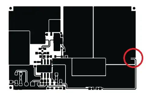
Top Copper from TPS40200 evaluation module

Michael Shaw
  • 163
  • 4

1 Answers1

8

No, I don't think it's a filter, I think it's used for the voltage feedback line and this is a way to make sure that the voltage on this feedback line is the "real" voltage on this large copper area and that is not disturbed by the currents through the components connected to this copper area.

Bimpelrekkie
  • 80,139
  • 2
  • 93
  • 183
  • 2
    I agree on this. @Michael look at the end of the datasheet it's written that feedback resistance should be away from big currents circuit. And the resistance down the board is the feedback one if you look at the placement and at the datasheet of the eval board. – damien Oct 28 '15 at 16:06
  • Thanks, this makes a lot more sense than what I was thinking! – Michael Shaw Oct 28 '15 at 16:22
  • @MichaelShaw I don't think your considerations were overly off. It does look a lot like the things you do on patch antennas (which also are but large copper areas on a PCB) to match RF line impedance. – Marcus Müller Oct 28 '15 at 21:40