10

I'm attempting to route a simple board, the first I've done in 15 years since I routed a 12V linear power supply in the equivalent of mspaint. This board consists mainly of an LPC2387, which is an LQFP100 IC that requires a variety of +3.3V and GND connections.

As I play around with routing the traces for this thing, it strikes me that even with only GND routed, the underside of the IC is it's own little rat's nest of traces. Using this strategy, I'm going to need a giant pile of vias under there just to power the IC.

Is this normal? Am I going about this all wrong?

enter image description here

Brian Carlton
  • 13,252
  • 5
  • 43
  • 64
Mark
  • 4,650
  • 10
  • 48
  • 53
  • 2
    How do you plan to fab this board? Most importantly, how many layers do you intend to have? Vias are only a problem if you have only one effective layer to work with, or are drilling them yourself. (Also, a hint which will hopefully be expanded by other users: Copper pour. Try typing `polygon GND` in the command bar and make a rectangle around your IC, then type `ratsnest`) – Kevin Vermeer Sep 19 '11 at 19:24
  • Hopefully 2 layers, and it'll be sent to a fab house to fab (something like BatchPCB), so vias aren't a problem. I've just never seen anything like this before (though I haven't looked hard). – Mark Sep 19 '11 at 19:40
  • 2
    You should avoid those acute angles between tracks, they can cause problems with etching. You also need to decouple every power-ground pair. – Leon Heller Sep 19 '11 at 20:04
  • 1
    There are a lot of VCC/GND pairs because that chip needs a very low impedence path to power and ground. You should put a cap on every pair, if possible (usually on the back of the board behind the uC). Skip these and one side of the chip may 'starve' the other. A 4 layer board with dedicated power and ground planes would be way, way better. – darron Sep 19 '11 at 20:05
  • Are 90 degree angles allowed? Common wisdom seems to be avoid-if-possible... – Mark Sep 20 '11 at 04:11
  • @Mark - 90 degree angles can (but are less likely to) create the same acid traps as more acute angles. If you T-junction your traces, you should make a miter or radius at the junction such that every angle between thin traces is 135° or greater (Note: This is not mandatory for 90 degree traces. For acute angles, it is). In this case, though, you'll probably be joining them to a plane. – Kevin Vermeer Sep 20 '11 at 12:52

2 Answers2

9

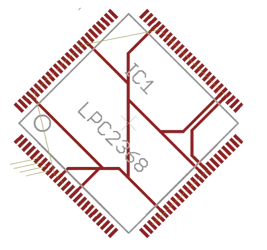
What you're missing is the use of a power plane. It appears you're using Eagle, use the polygon command to create a plane, and name it GND. Then, use the ratsnest command to pour this plane over your board.

For a 4-layer board, you should have an internal GND layer and an internal VDD layer. Route your signals on the outer layers, and pass vias through to the planes near the pads.

For a 2-layer board, the issue becomes more complicated. It's quite easy to set up loops (which are bad for signal integrity and EMI) when routing signals through a power layer.

The IOIO is an example of a 2-layer design with good routing. The bottom layer in this image is GND; I've edited this to use a 3.3V plane under the IC instead of their original traces. You can get the un-edited orignal documentation (including layout files) here.

layout sample

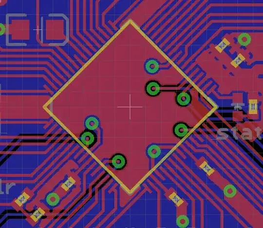
They placed the decoupling caps rather far away. Presumably, this was done so that all parts could be placed on the top layer. If you can solder on both sides it's probably better to locate them directly under the IC, and connect with short vias to the associated pins.

Also note that their voltage regulator and its associated 10uF decoupling cap are barely off-screenshot to the right. If they were any further, I'd also add a bulk cap of 10uF or so immediately under the IC, in addition to the 0603s shown.

Finally, note that even though there's a large, low-impedance plane under the IC, it's fed by two 8 mil traces under two pads at the right side. If I was being extra-careful, I'd have moved the LED and resistor at the right, as well as the 5V trace coming in across the right corner, to get a lower-impedance connection through that gap.

Kevin Vermeer
  • 19,989
  • 8
  • 57
  • 102
3

Connect them to the VCC/GND planes near the pins. Quieter power connections, more room to route the rest.

Kevin Vermeer
  • 19,989
  • 8
  • 57
  • 102
Brian Carlton
  • 13,252
  • 5
  • 43
  • 64