0

A couple of years ago I read an interesting Wikipedia article about something called a "field-programmable gate array". The article made it sound like it's a box of logic gets which you can arbitrarily wire together to implement any kind of logic you want (but without needing thousands of discrete components).

Now, I had assumed this works something like a PROM. As in, you buy a die which has all the gates on it, with everything connected to everything, and then there's a glass window to the die, and you use one of those extremely expensive UV-laser writers to "burn" through the connections you don't want, resulting in the logic circuit you designed. (And maybe there's a version that's erasable too, like how CD-RW is somehow erasable.) Once you've "burned" your program into the chip, it behaves as if it were that actual combination of logic gates. (Because now it is that combination of logic gates!)

However, more recently I've been reading about this, and it appears this isn't how the technology works at all. A lot of recent articles talk about needing to send a "bitstream" to the FPGA at system power-up (and even the possibility of encrypting this bitstream to stop your competitors reading it). This makes it sound alarmingly like a FPGA isn't a hardware construct at all; it makes it sound like really it's just an ordinary microprocessor that's simulating your design in software.

In particular, that means a design programmed into an FPGA can never run any faster than the underlying microprocessor that's simulating it. Which kind of makes the entire endeavour sound... kinda pointless. I thought the whole point of an FPGA was to make custom logic that does stuff faster than you can do it in software. But all this "bitstream" stuff makes it sound like it is still software...

I'm a little confused here. How does an FPGA actually work?
MathematicalOrchid
  • 1,701
  • 2
  • 18
  • 23
  • What they mean is that you need external non-volatile memory to save your program, usually EEPROM or FLASH. And on the startup (when power is applied to the FPGA and memory) FPGA reads the program from the external memory and changes its internal logic. – Golaž Oct 07 '15 at 10:31
  • How does it "change its internal logic" electronically? What, a giant array of switches or something? – MathematicalOrchid Oct 07 '15 at 10:36
  • 2
    Lots of information is available via Google. Question should be closed. – Leon Heller Oct 07 '15 at 10:45
  • @pjc50 That question seems to be about what a FPGA does, whereas I guess I'm asking how it does it? – MathematicalOrchid Oct 07 '15 at 11:17

4 Answers4

4

It is a giant array of switches, yes.

Specifically, an FPGA cell will usually have one state element (D-flop) with a lookup table (LUT) on the input. The LUT is programmed to give a particular output for each possible combination of inputs.

Additional switches connect the cells to a routing network of wires. There are usually also a number of specific-purpose blocks for doing common operations like additions and multiplications, small memory blocks of (say) 1kb each, and high-speed transceivers for doing things like Ethernet or PCIe.

It really isn't like a microprocessor and does deliver large amounts of single-cycle logic in parallel. However for integer non-parallelisable tasks a regular CPU may have higher throughput, or for the very specific workload they are designed for GPUs are faster.

FPGAs give you low-level access to signals with low, fixed, latency. That's their real value.

pjc50
  • 46,540
  • 4
  • 64
  • 126
3

The FPGA is indeed a big bag of gates. However (in many of the popular varieties, there are others) the gates are wired together with multiplexers, whose routing data is provided by static RAM storage. This means the gates do have a static path from one to another, and they will execute parallel logic at the full speed you would expect.

When it's first turned on, there's an initialisation phase, where some extra dedicated logic in the FPGA reads a memory, and sends all the programming bits to the multiplexers. During this time, the I/O bits can be programmed to be high impedance.

Neil_UK
  • 158,152
  • 3
  • 173
  • 387
2

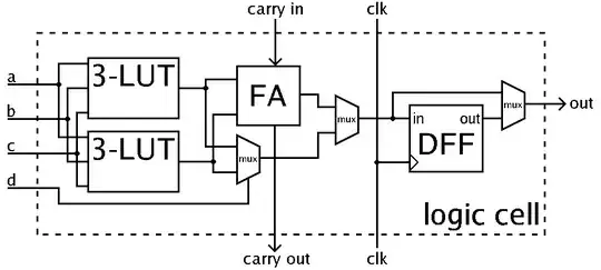
FPGAs consists of a number of "Logic Blocks", which can have things such as look-up-tables, registers (flop-flops) and usually some other logic, that enables them to be easily configured to commonly used elements, such as adders. The logic blocks have a few switches inside them that can disable certain elements (eg. the flip-flop). This and the look up table for the LUT is configured by the bit-stream. You can see a simple Logic Block here:

A sketch of a simple Logic Block from wiki

The FPGA might also have some special Logic Blocks, like multiplication blocks, output blocks, clock management blocks, etc.

The inputs and outputs of the Logic Blocks are connected through a number of programmable interconnections, or as you say " a giant array of switches", except that the size of the array has been minimized, so that only Logic Blocks close to each other (on the same bus) can connect. Usually there will be interconnections where buses can connect directly, but it is not uncommon that routing through a LB is necessary.

Being able to reconfigure the "switches" in the LBs and re-configuring the programmable interconnections, ether at "boot" or in some instances during run time, i exactly what makes the gate array field programmable.

While searching for images i stumbled on this good description on the internal workings of an FPGA.

Skrogh
  • 46
  • 2
  • So #1: it's not just simple logic gates, and #2: there are extra logic gates purely for routing signals around. (?) – MathematicalOrchid Oct 07 '15 at 11:10
  • #1: Correct, i found a [pdf](http://www.ece.ubc.ca/~edc/464/lectures/lec6.pdf) that explains the difference between PAL, CPLD and FPGA (PAL are pure "logic gates") #2: Yes, well more like a simple CMOS switch connecting two wires. – Skrogh Oct 07 '15 at 11:25
0

Your understanding above about the logic functionality is correct. But your understanding of the programming is incorrect. A Field Programmable Gate Array is indeed a giant array of logic elements connected by a bunch of routing switches. The routing switches are configured at power on, and because of this *Most FPGA's require external non-volatile storage to contain the "bitstream" which gets read in at power on.

The fundamental logic elements you see in an FPGA are typically a 4 or 6 input Look Up Table, fed to a 2 or 4 D Flip Flops, and some MUX'es to allow bypass of some or all of the above. These "Configurable Logic Blocks" (CLBs) are then connected in a giant sort of interconnected matrix. With a 6 input LUT you can implement any 6 to 1 combinatoric logic, and with D Flops, you can implement memory which with combinatoric logic enable one to implement sequential logic. Newer FPGA's also contain additional specialized hard Logic elements such as 48-Bit Multiply Accumulate Units (MAC's), Specialized High Speed I/O resources.

The Interconnect switches between CLBs as well as the control lines that go inside each CLB are all addressed and controlled by an internal non-volatile configuration memory which is accessed by a piece of logic called the Configuration Access Port. at Debug time, you use JTAG to write the bitstream to the CAP. At deployment time, at power on, the non-volatile external storage is read and written into the CAP. Most FPGA's are able to both self configure (i.e: at boot, they clock and address the external memory) or be configured by an external controller (i.e: something other than the FPGA does this process).

The design flow generally entails you specifying your design, then 3 or 4 steps of what might be called compiling. The later steps are sort of amorphous and sometimes of little concern to the designer (but that can become very important depending on your design.) The first step takes your VHDL and turns it into either RTL or some other netlist, that is strictly speaking "logic that can be implemented," then the next step (Mapping) sort of maps your netlist into a FPGA-vendor/family-specific, but device-generic, sort of infinite grid of CLBs, then the next step(Translating) translates that into a grid of actual logic elements, then in the next step (Placing and Routing) that grid of logic elements in fit into the grid of the actual model number device you are using, which is the first point in the process that any specific part of your design is actually correlated to a physical addressable piece of logic. Placing and routing also handles ensuring that the timing of your design is met.

Botton line, FPGA is not logic simulated by a program. FPGA is reconfigurable synchronous digital logic, that subject to physical limits of rise and fall time, and propagation delay, will run as fast as you clock it.

Jotorious
  • 659
  • 3
  • 10