5

So far I see some JEDEC standards for part packages, but I need standards for the corresponding footprints. For example MS-026 is a JEDEC standard for a PQFP part, so what would be the standards that covers the foot print for this part?

Just a note, I started looking for this after seeing a few datasheets' recommended layouts that were smaller than the pins on the part.
bitsmack
  • 16,747
  • 9
  • 52
  • 108
Jason
  • 302
  • 2
  • 9
  • Generally manufacturers will provide their own reference footprints. They may reference a jedec standard but with a disclaimer. The jedec footprint would be generic based on recommended clearances and tolerances for a standard jedec compliant package (with its associated tolerances) – crasic Sep 23 '15 at 17:20
  • @crasic, the part vendor's footprints should only be taken as a starting point. They don't know what assembly shop you're using, whether you're doing wave or reflow solder, what kind of solder paste, what stencil thickness, what thermal loads are near where you placed their part, etc. etc. Usually their recommendations are okay, but your assembly shop will be able to give you a better recommendation, if they are having trouble with a particular part. – The Photon Sep 23 '15 at 17:46
  • @ThePhoton agreed, the only sure fire way is to go through the DFM process with your preferred manufacturer, however hobbyist and low-cost shops tend to spin a board as-is after conforming to their tolerances especially if they aren't doing the PCBA. I've also had the experience of a full production board house doing their DFM verification against the manufacturer recommended footprints almost verbatim – crasic Sep 23 '15 at 18:36

1 Answers1

8

It's the IPC-7351B - "Generic Requirements for Surface Mount Design and Land Pattern Standard"

The document only provides recommendations; there is no enforcement. However, more and more manufacturers seem to be using it to inform their footprint suggestions.

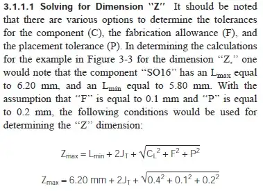
Note that this spec isn't easy to use directly. Instead of tables of land pattern dimensions, you see sections like this (take from a previous version of the spec):

....ipc

Instead, I use a software called Library Expert. It's free and quite useful. It creates footprints to the IPC-7351 spec. It will actually build up the symbols for a number of software packages, e.g. Eagle, OrCAD, Altium, and others.

bitsmack
  • 16,747
  • 9
  • 52
  • 108
  • +1 I've been using the older LP Calculator and wasn't aware of Library Expert with all the CAD support. See also: http://landpatterns.ipc.org/default.asp – Tut Sep 23 '15 at 18:58
  • Also IPC-SM-782 covers a bunch of footprints. – Jason Sep 23 '15 at 22:31
  • BTW, does IPC-7351B cover most common packages? The PCB Library Expert FREE Viewer doesnt have many diode packages, and the IPC-SM-782 doesnt have the DO-214 diode packages. – Jason Sep 23 '15 at 22:36
  • @Jason I've updated my answer, please take a look. – bitsmack Sep 23 '15 at 23:01