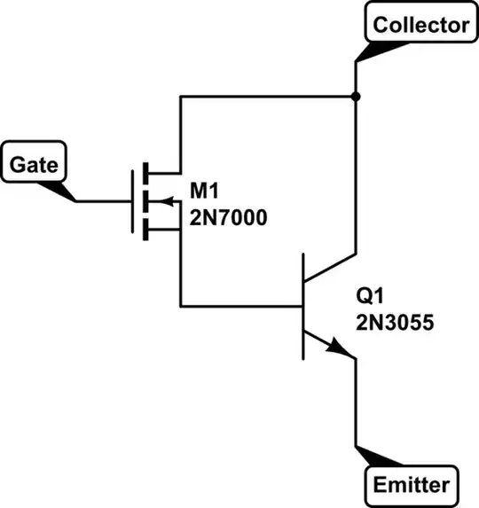
The circuit is interesting .I did the same basic thing with a MPF102 Jfet in a plastic to92 package and a BD139 BJT in a to126 package.My idea of doing this was to preserve the Analog input characteristics like low capacitance of the FET and get the power dissipation of the to126 package.The aggregate handles more current and hence power but not voltage.YOUR circuit is valid because you wouldnt be able to get a big mosfet with such low gate source capacitance.Switching performance would be terrible at turnoff in fact it would be worse than an IGBT because you have no base emitter resistor and in effect the IGBT does .Compared to an IGBT your circuit will have less input capacitance .Also you have more control over switching performance because the base and emmiter of the BJT are both accesable.Finaly your circuit wont ever latch up! like some IGBTs are rumoured to do.