25

In a moment of cheapness, I decided not to order a 5v to 3.3v level shifter from Sparkfun, but instead to put it together myself. The original schematic used a BSS138 MOSFET, but since I enjoy surface-mount soldering about as much as root canal treatment, I decided to use a similar seeming MOSFET that is through-hole mounted and easily available from my preferred supplier.

The results of this were sub-optimal. When pulling the 5v line to ground, all was fine - the 3.3v side went to 0.07v. But when pulling the 3.3v to ground, the 5v line showed around 4.14v (it was otherwise a touch above 5.1v). On a closer reading of the datasheets involved, as well as the original Philips application note on the subject, I began to come to the conclusion that the gate threshold voltage was the problem.

By altering the schematic and tying the MOSFET's gate to 5v instead of 3.3v, both sides seem to work fine. Pulling either side low causes the other side to go low. I'm not, however, at all confident that this is actually a sane thing to do. My understanding of the original schematic isn't deep enough to form a sensible opinion.

Will this modified schematic work, or are the current good results I'm seeing mere fluke or a precursor to something releasing magic smoke?

Jon Bright
  • 635
  • 2
  • 7
  • 9

1 Answers1

49

Short answer

  • In this circuit Vth (the gate to source voltage at which the MOSFET is just turned on) is crucial. Vth should be substantially lower than Vh-Vl = 5V - 3.3V = 1.7V.

    The BSS138 has a Vth of 0.8 / 1.3 / 1.5 min/typical/max.
    So while notionally it would be "good enough" here as 1.7>1.5, that margin is uncomfortably small.

    Unfortunately, the alternative that you chose is even worse than the BSS138.
    The FQN1N60C has a Vth of 2/-/4 V. ie at its best case Vth of 2V it is higher than the required 1.7V and it can have a Vth of as much as 4V which is vastly more than 1.7V in this application.

    An acceptable (just) TO92 MOSFET in stock at Digikey is the Zetex / Diodes Inc ZVNL110a.
    This has Vth of 0.75/-/1.5 Volts. This is about the same as the BSS138.


Longer:

  • The BSS138 is a, relatively, hunk of junk. It has its place but it is stretched beyond its safe capabilities in this circuit. Unfortunately, the alternative that you chose, a FQN1N60C, is even worse.

  • Your raising voltage LV to a voltage equivalent to HV overcomes the FQN1N60C's high Vth value.

The reason your original circuit works poorly is because the FQN1N60C is a very sorry specimen of the MOSFET art, and the reason that your revised circuit works well is also because the FQN1N60C is a very sorry specimen of the MOSFET art. A low Vth MOSFET would work properly in the original circuit and fail in the revised one.

This is because in the original circuit the FQN1N60C Vth is too high for the available Vth and is not turning on properly. A MOSFET with low enough Vth would turn on properly with the available voltage. In the revised circuit you have provided the FQN1N60C with enough gate voltage in the operated state but not so much that it will be operated unintentionally. If you used a low Vth MOSFET it would be turned on by the fate voltage available when it was meant to be off and the circuit would fail.

The circuit is an extremely clever one BUT it's cleverness depends on the MOSFET having enough gate voltage to drive it when TX_LV is low but not enough voltage to drive it when TC_LV is high. Usually LV = T_LV when TX_LV is high, so the MOSFET sees no gate voltage. By increasing LV to HV you provide a gate voltage of (HV-LV) when TX_LV is high. As HV-LV = 5-3.3 = 1.7V the FQN1N60C does not false trigger as it's practical Vth is > 1.7V.

Below is the original level shifter circuit diagram.

The BSS138 is an N Channel MOSFET - so it conducts when its gate is positive relative to source, it is usual for it's drain to be higher than it's source, and the internal body diode blocks when Vds is +ve and conducts when Vds is negative.
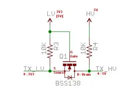
enter image description here

Normal operation
With TXLV and TXHV high, gate is at LV (originally 3V3, source is at TX_LV = 3.3 so Vgs=0 so FET is off.
Source is at TX_LV pulled there by R3.

Send logic 0 left to right.
Pull TX_LV low. Source = 0V, gate = 3V3. So Vgs = 3V3. As this is > Vth BSS138 is turned on. As source = 0V and FET is on, TX_HV will be also pulled to low. That was easy :-).

Send logic 0 right to left.
Pull TX_HV low. Drain = 0. Gate is 3V3 via hard connection.
Source = 3V3 (but see below) So: Vgs = 0. FET is off. Vds = - 3V3.
BUT the BSS138 has an internal diode S to D. This diode will now conduct, pulling TX_LV down to a diode drop above TX_HV.
Also easy.

NOW replace BSS138 with FQN1N60C.
MOSFET's Vth is> to >> 1.7V margin between 5V and 3V3.
Now, in sending logic 0 LEFT TO RIGHT, grounding source gives Vgs = 3V3 = < 4V worst case. If true Vth is somewhere around 1.7V the circuit will sort of work.

Raising LV to 5V works as now Vgs = 5V.
BUT when TX_LV is high there is still 5-3.3 = 1.7V drive to MOSFET, even though it should be 0V, and was before.

If you now replace the MOSFET which has a Vth < 1,7V it will always be turned on. ie a better quality MOSFET works worse (or not at all). The "cure" is to use a MOSFET initially with Vth < to << 1.7V.

try-catch-finally
  • 1,254
  • 3
  • 19
  • 37
Russell McMahon
  • 147,325
  • 18
  • 210
  • 386
  • That's the second super-awesome answer you've given me in the past couple of days. Thank you very much for your help! – Jon Bright Aug 20 '11 at 14:28
  • @Russel - Strange that you didn't mention the "logic level" classification of FETs anywhere in this answer... – Kevin Vermeer Aug 20 '11 at 15:02
  • 1
    @Kevin Vermeer - I considered it for a scant moment. If I'd used it it would have been to say that it's a very subjective term - not quite marketing jargon but closer to such than is comfortable. And in this case there are two "logic levels" involved. The BSS138 is claimed to be "logic level" and it's bearably so on 5V and super marginally so on 3V for currents near its rated max. The reason it sort of works in this application is that Vth is typically typical and not worst case, and because currents are small. Instead I was specific about what Vth's were expected and acceptable. – Russell McMahon Aug 20 '11 at 21:19
  • 3
    I do not think that vh-vl > vth matters. I think what only matters is Vl > vth (note this is also conclusion of your analysis if I am reading it correctly) – mazurnification Aug 22 '11 at 15:11
  • Did anyone tried to pulse 5V 20MHz square wave in and get a reasonable 3V SQUARE wave out? – Nazar Mar 28 '14 at 18:28
  • Very good answer and explanation ! Good work !! Well, at least in this specific case a also think that the most important is that: Vl > vth. I even used the 2N7000 type and got excellente work connecting my arduino uno to the MMA8432Q accelerometer. –  Apr 06 '16 at 18:04
  • @naz This circuit only works for very low frequencies. 20 MHz is too much. – Pål-Kristian Engstad Apr 06 '16 at 20:17
  • 4
    I generally try hard to avoid succumbing to the temptation to call people "morons" online (or elsewhere) even though the term has a good formal meaning* and is apposite on occasions. Somehow 2 points were taken off this answer this week and it has 1 downvote. The loss of "rep" is of course utterly unimportant but its sad to think that there is a moron on this list who really thinks this answer is "not useful" given all available info. A question may have helped the doubter more. | *Moron = IQ 50-75. Apposite in area of discussion if not in all life areas in some cases, such as this one. – Russell McMahon Jun 12 '16 at 12:44
  • Your are mistaken about Vh-Vl>Vth. It is in fact Vl-Vdiode that must be > Vth. See [here](http://www.hobbytronics.co.uk/mosfet-voltage-level-converter) for principle of operation. – rustyx Mar 03 '19 at 22:48
  • @rustyx 7+ years on :-). It's complex. problem is that I did not pedantically enough spell out the conditions under which various situations applied. I think that by adding more appropriate qualifying words the explanation may be clearer. || The principle of operation that I explained and that was given in your reference appear 100% identical(not of course in the exact words but in mechanism) - as I'd expect. If you can see any substantive difference that I've missed I'd be happy to hear of it. ... – Russell McMahon Mar 04 '19 at 03:37
  • | If by Vh, Vl & Vdiode you mean : Vin_left high & low and Vdiode_fwd_conducting then you'll need to spell out your related argument. – Russell McMahon Mar 04 '19 at 03:37
  • @rustyx a few hours on. re " ...Your are mistaken about Vh-Vl>Vth..."-> No. Expanding: ' For left to right operation assume Vh = input high =~ LV (3V3 here) . Assume input low = Vl. Vl MAY be zbout zero but MAY be higher. Gate is at LV - here = 3v3. When source is at Vh then vgs = LV-VH. This is either 0 or very low. FET is off. | When Vin = Vl = low then FET sees Vgs = LV-Vl. = Vh-Vl. If Vh-Vl is < Vth FET will not turn on. If Vh-Vl is >> Vth then FEt turns on fully and no problem. If Vh-Vl only slighty higher than Vth then FET is sort of on and cct sort of works. Hence my statement. – Russell McMahon Mar 04 '19 at 06:16
  • @RussellMcMahon Your reply is very detailed and easy to understand. There is one thing I'm wondering. What determines the maximum possible HV? AdaFruit sells a module based on this design, and it says HV is 10V max. I've read the BSS138 datasheet and couldn't determine what would prevent down-shifting from 12 or even 24V. Can you explain please? – Gene Pavlovsky Nov 18 '20 at 00:06