0

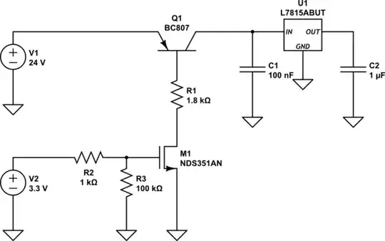
I'm trying to run a OLED display densitron with a ssd1322 controller. It requires basically two supply voltages 15V VCC supply and maximum 3.5V Vci supply voltage for operation and IO pins. There is a power sequence that need to followed, so that when we turn on the display first come the Vci and after some small time VCC from GND. When we turn it off first is the VCC to be grounded and then is the Vci. For that purpose I need to design a e-switch controlled by a microcontroller in my case stm32f373R8. It should be an upper switch, meaning that it should not leave the GND open when it is switched off, because that will damage the voltage regulator. Basically here is what I have:

schematic

simulate this circuit – Schematic created using CircuitLab

Where the voltage source V2 is the port of the microcontroller. Since I got this schematic from the datasheet of the voltage regulator, I have the following questions:

  1. Aren't the transistors Q1 and M1 forming a controlled current source? The current that will flow through the base when M1 is on will be around 12.7 mA. Then the output current is around 1.27 A:

schematic

simulate this circuit

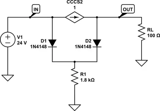
  1. How the resistor R1 is controlling the emitter voltage?
  2. In the case of V1 is 3.3 V I notice a voltage drop at the U1 input of 2.5 V instead of the 3.2 V. Why?
  3. When I experimented with the real PNP transistor I noticed that even when NMOS is off at the input of U1 there are 10V measured. Would you explain the physics behind? Is there a way to eliminate that voltage?
  4. How can implement the same switch but with PMOSFET, instead of PNP?

Thanks in advance!

judoka_acl
  • 389
  • 4
  • 16
  • you may update M1 symbol – User323693 Jul 14 '15 at 09:35
  • M1 and Q1 is just a switch. R1 limits the base current. What is the maximum collector current of q1? – User323693 Jul 14 '15 at 09:58
  • @Umar why may I do that? – judoka_acl Jul 14 '15 at 09:58
  • M1 symbol you mean? It is a PFET symbol right? – User323693 Jul 14 '15 at 10:00
  • No. It's a **M**OSFET symbol. The maximum collector current is 500 mA. – judoka_acl Jul 14 '15 at 10:54
  • i meant PMOSFET, Source arrows comes inside for that... Since you are only able to turn MOSFET on and OFF, there is no control over base current. It is simply a switch for voltage of 24 V at 500 mA of maximum current. Do you just need to control input to U1 via V2? – User323693 Jul 14 '15 at 13:11
  • Yes, I need to control input to U1, so that when V2 (which is a port of uC) is 0V then U1 has as input 0V, when it is 3.3V then U1 has as input 24V. I know it is simply a switch for voltage, because I have tested it already on a circuit and it's working very good. The question is how this is a voltage switch, when according to the simple pnp model it should be a current switch. In other words if we put a load resistor in place of the U1, no matter what is the resistance the voltage will be around V1 when M1 is on. How? – judoka_acl Jul 14 '15 at 13:19
  • The BJT is on full saturation now since base current is huge. The BJT presents about 100 mV or less drop acroas it. It is like a physicsl turned on switch. isn't it? If tou replace the transistor with a switch in your first circuit, you are actually probing across C1 which is nothing but V1 when V2 is 3.3 V. Does it make a point? – User323693 Jul 14 '15 at 13:35
  • What about when V1 is 3.3V? Why I have 2.5V at the output? – judoka_acl Jul 14 '15 at 14:28
  • Now the base voltage(and hence current) is being reduced. Earlier it was (24 V - 0 V)/R1. But now, it is (3.3 - 0 V)/R1. The reduced base current is less and hence the transistor is no longer in saturation. The remaining 0.8 V will be across Vce, which can also be verified by looking at the graph of Vce vs Ic for various Ib in the BC807 datasheet – User323693 Jul 14 '15 at 14:39
  • Very good. @Umar thank you for this simple and clear explanation. Could you elaborate on 4 and 5, please. – judoka_acl Jul 14 '15 at 15:01
  • http://electronics.stackexchange.com/questions/177056/using-arduino-mosfet-to-automate-the-pressing-of-button for sl. No 5. For #4 I suggest you to place a kilo ohm valued resitor between BC807's Base and emitter. Don't let the base float. I am on mobile now and can give some circuit once I get a computer – User323693 Jul 14 '15 at 15:36

1 Answers1

0
  1. MOSFET M1 and Transistor Q1 forms a High side switches. The Base current for Q1 is sufficient to drive the Q1 into saturation. Hence it will be only a ON or OFF switch.
  2. R1 is only controlling the base current for Q1. Higher the value, lower will be the maximum collector current allowed.
  3. When V1 is reduced, the base current drops to 1.3 mA (3 - Vbe)/1.8k, which is way less to drive the transistor to saturation. The Vce drop for corresponding base current (Ib) can be observed from the figure 10 or 11 from the datasheet of BC807.
  4. Placing a pull up resistor (ex.: 4.7k) between base and emitter will avoid accidental turn on when base is left floating (V2 is OFF or 0 V). The resistor will not impact the turn on characteristics much, as the voltage across the base and emitter will be held at max of 0.8 V by the PNP transistor.
  5. Similar answer here
User323693
  • 9,151
  • 4
  • 21
  • 50