How does NPN transistors actually work? In the picture below, I understand that electrons flow in A as the n-p junction of the Emitter and Base is forward-biased. However, the p-n junction of Base and Collector is reverse-biased, so how does the electrons in B flow?
-
Do some youtube search, there are some people that explain it quite ok there, as it works best with some images. – PlasmaHH Jun 30 '15 at 12:13
-
A very simplistic view on this: The E-B junction is in forward, the B region is very narrow/short. So electrons that happily cross the E-B junction get too close to the collector and are sucked into it (the collector). As I said, this is a simplistic view, not scientific in any way but maybe helps you to understand. Dave Jones is the man you need to see: https://www.youtube.com/watch?v=qUeK7pHe0rI Just watch that video (and all his other videos as well) and become a 1st rate engineer :-) – Bimpelrekkie Jun 30 '15 at 12:16
-
1Such questions that can easily be answered with a Google search are closed. – Leon Heller Jun 30 '15 at 12:45
-
If you really want to know how it works, I suggest starting with a good book on Solid-State physics. I used Kittel, which dates back more than 50 years. If you just want to design circuits, you should study the characteristics. – Spehro Pefhany Jun 30 '15 at 16:01
2 Answers
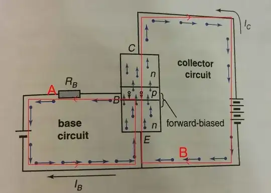
Very short (and incomplete) explanation:
There are many things to understand first but I think the most important thing is to know that currents can be differentiated by their cause:
Drift current is caused by a gradient of the electrical field (voltage).
Diffusion current is caused by a gradient of concentration of carriers (i.e. electrons or holes).
Minority carriers (electrons in the p-region) reach the collector by diffusion (→ diffusion current). It requires the base to be thin enough that only a small percentage of minority carriers are lost by recombination (i.e. thickness of base << diffusion length; that's why it doesn't work with two discrete diodes connected back to back).
To understand the whole process I suggest to understand drift and diffusion current, minority carriers, diffusion length, recombination, pn-junction, ...

- 16,043
- 34
- 43
In short:
B-E junction is forward biased and causes electrons (better: negative charges) to move from the emitter (it "emittes") to the base region (forward biased pn junction) which is very thin.
Therefore, the majority of the carriers has enough energy to cross this depletion area and will be "collected" by the collector potential which is larger than the base potential (that means: The C-B junction is reverse biased). This is the collector current.
A (small) rest of the charged carriers forms the base current.
Therefore: The B-E voltage causes the emitter current IE which is split into the collector current IC and the (small) base current IB: IE=IC+IB.
That means: The voltage VBE controls/determines both currents: IC and IB. And the ratio IC/IB is nearly constant (called "current gain").

- 24,857
- 2
- 23
- 52