1

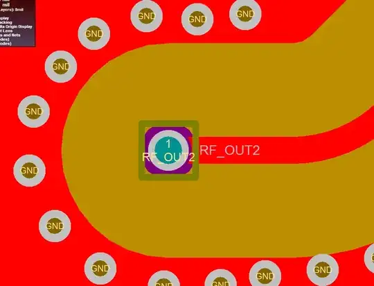
I'm routing an RF board ( above 1 Ghz) with microstrip lines. Our plan is to feed it from the backside, take it through the via onto the top layer and continue routing. as part of our rules we pull back the ground copper pour to ensure microstrip behavior.

Should we do the same for the other layers the via passes through? Or is the patristic capacitance low enough to not worry about? Or would the patristic capacitance cancel out the inductance of the via?

what a via

Legen Diary
  • 480
  • 4
  • 16
  • In my experience, best to experiment. Make up a small board with 10 different attempts, and measure them all. I've had good results with some additional capacitance on the signal layer, using a larger pad or extending the microstrip beyond the via. But intermediate layers should not get too close, I'd pull them back several times the layer thickness. – tomnexus Jun 16 '15 at 22:22
  • 1
    Looks like a good candidate for simulation with a 3d field solver – Some Hardware Guy Jun 17 '15 at 00:12
  • Can you provide your PCB stackup? Effects will be vastly different between 0.1mm and 1.6mm layer distance. – corecode Jun 17 '15 at 08:14
  • @SomeHardwareGuy wish i had the time... – Legen Diary Jun 17 '15 at 20:11
  • @corecode I can't say exactly what the stackup is, but it is closer to 1.6 than to .1 – Legen Diary Jun 17 '15 at 20:11
  • 1
    @LegenDiary without stackup information you will not be able to get a correct impedance. – corecode Jun 17 '15 at 21:02
  • If you have access to an RF schematic tool like Microwave Office or Agilent ADS they usually have a schematic element that models such an effect. – DakotaD Jun 18 '15 at 13:04

1 Answers1

1

I would suggest treating the transition like an offset or eccentric coaxial line with the signal via being the center conductor and the ground vias the outer shield. Place the ground vias as close together as possible for the best performance. Also pull back all internal layers so that they are shielded by the ground vias.

DakotaD
  • 791
  • 2
  • 5
  • 13