8

I am working with boost converters recently. I have problem which you can find here. After going through the datasheet several times I encountered the special focus on the ground plane. It talks about different ground nodes. I have no idea what it means. I would be grateful if someone can point out what is the best practice as well. Any suggestions would be appreciated.

Extract from datasheet regarding layout

My revised layout:

PCB layout

Circuit diagram:

  • C1 ceramic 10% 2.2uf
  • C2 ceramic 10% 4.7uf

  • L1 1uh 1206 package

circuit diagram

Arjun
  • 680
  • 5
  • 24
  • 2
    I suggest that you look at "TPS61240EVM-360 User's Guide" I also suggest that you refer http://www.smps.us/power-supply.html – Mahendra Gunawardena Jun 16 '15 at 10:41
  • @MattYoung presumably because it allows direct access to the Vin/Gnd and Vout/Gnd busses. – David Freitag Jun 16 '15 at 15:02
  • @MattYoung definitely a possibility, but if either J1 or J2 were jumpered I would find it difficult to imagine there would be a voltage of 1.8V-2.2V would be present on Vout. – David Freitag Jun 16 '15 at 15:07
  • @DavidFreitag I see now, was thinking this was a smaller block in a larger system rather than a single board. It's just a poorly drawn schematic. – Matt Young Jun 16 '15 at 15:09
  • I am sorry for the schematics. This converter is just a small part for my project. I need to meet the deadline. I do not have access to electronic shops, it takes me more than a week even if i ordered through DHL. so there is no way i could replace it with alternatives. :( :( – Arjun Jun 16 '15 at 15:40

3 Answers3

8

It's suggesting that there is a "star-point" that "power ground" and "feedback/control ground" use as their points of reference to 0V. Anything that should/must connect to power ground i.e. input decoupling caps, output decoupling caps and main ground on the chip should be separate from ground on the feedback potential divider (not used on your design). These two separate grounds should make just one connection to each other and this is called the "star-point".

This ensures that load currents and input currents (that might create millivolts of volt drop on their track) do not influence the voltage that the feedback resistor network measures. If these currents did influence the feedback resistors, then you can expect a noisy output and possible instability.

The "star-point" is, by default, right at the main 0V connection for the chip.

For buck regulators (using a fly-back diode), this diode should be naturally on the power ground and NOT connected to the control ground. Several other pins may need to use the control ground and these include, soft-start input capacitors, oscillator resistor and capacitors and incidental digital inputs (such as external switching clock if used).

Andy aka
  • 434,556
  • 28
  • 351
  • 777
  • Can you tell me whether the revised layout is good or not? I am only getting 1.8v to 2.2V from two alkaline battery(3.2V) – Arjun Jun 16 '15 at 12:16
  • I have no idea what the circuit is. – Andy aka Jun 16 '15 at 13:38
  • Its just a 'take lower input voltage, throw higher voltage circuit' :D, I am just curious about i am good with ground or not? anyway thank you very much – Arjun Jun 16 '15 at 14:28
  • 1
    I refuse to analyse a PCB without a circuit diagram. That's not me being stubborn BTW. A PCB layout without a schematic is guesswork. – Andy aka Jun 16 '15 at 14:32
  • I have added the schematics too :D – Arjun Jun 16 '15 at 14:36
  • I realize that it is probably an unsuitable drawing package but it looks like the inductor is directly connected to EN instead of Vin. Also EN needs to connect to Vin. I guess if there should be a dot where the wires cross it makes sense and the layout then becomes clearer. I think it will be OK. – Andy aka Jun 16 '15 at 14:45
  • I am sorry my bad, VIN, EN and L are connected. – Arjun Jun 16 '15 at 14:58
3

As always, I would suggest looking for a development or evaluation board when designing with a new device. It would appear that (after a simple google search) there is a TI eval board available for the TPS61240.

Any quality eval/development board will include schematics and generally a PCB layout (especially with devices such as switch mode regulators that are very layout-dependent). As it turns out, TI has great eval boards, and the datasheet provided with this one includes a full board layout and schematic.

The eval board can be found here on Digikey, and the pdf document here directly from TI. This design combines three TPS61240 devices on the same board (different packages etc). The section relevant to the part you appear to be using is outlined on page 7 as a schematic, and includes the section of the board layout with the parts U11, L11, C11, etc. I would recommend you closely study this design and use it as a springboard for your design.

Also, it's not necessary, but I also recommend purchasing one of these eval kits. In this case the eval kit is relatively cheap at $50 USD (if not from Digikey, you should be able to get it direct from TI), and it always helps to have a working circuit to probe with a scope when searching for bugs.

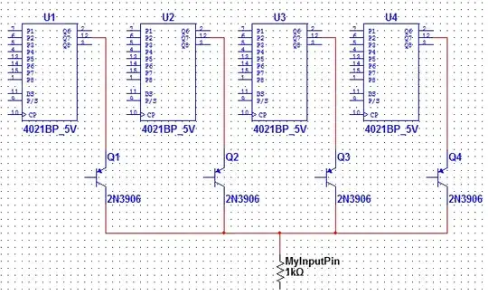
As an aside, I would also seriously recommend that you improve your schematic drawing. It's one thing to ask the community for help on your design, but it's a completely different issue when we need to decipher (sorry if this is a bit blunt) schematics that are as poorly drawn as the one you have provided. I can tell that you are using Cadsoft Eagle as it is the package that I use personally, and there is literally no reason for drawings such as this. Parts should have designators, names, and values. Quality drawings not only help us, but they help you in the long run whether you need to debug a circuit or reuse it for another project; all you need to do is take the time to do things properly. If you need an example of a good schematic, look up other various evaluation boards. It doesn't matter what function they serve, you are merely looking at the schematic to take cues.

David Freitag
  • 401
  • 1
  • 4
  • 14
1

Your new layout is a significant improvement over the old. Will it be enough? Only testing it will tell. If you still don't get 5v, you should try another set of components. Don't assume that they are good just because you got them from the manufacturer. Also make sure you installed them correctly (right place and direction). Good luck.

Guill
  • 2,430
  • 10
  • 6