12

I'm a hobbyist EE in college, and have been building breadboard circuits and perfboard circuits for the past year or so. I want to move on to doing PCB design.

I wanted to start with something small so I designed a small amplifier circuit for a microphone that I want to make into a module on a PCB.

Here is the file for what I designed in Fritzing (I went with this software because it's user friendly): http://www.mediafire.com/?2b2as7iibys68cu

Here is an image if you don't have the program:

pcb

Is this a good design? How can I improve it?

The general schematic I followed was this (in case you wanted to know):

sch 
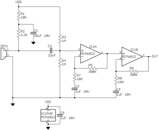
(Credit @Olin Lathrop)

What advice can you give me on getting started? Any resources you can recommend? What software would you recommend? Ideal would be free and easy to learn. What type of class would you suggest I take in college to get deeper into this?

Shubham
  • 6,054
  • 12
  • 41
  • 55

3 Answers3

17

I'll just comment on the design:

  1. Replace C5 with a 100nF ceramic capacitor and place it close to the power supply pin of the MCP6022.
  2. Put the designators on the PCB-Design, not values. Make it far easier to understand the layout.
  3. Avoid 90° trace bends, they can cause problems when etching the board. They're also bad for high-speed stuff (at least that's the common opinion on the matter). Use two 45° bends instead.
  4. Consider flooding one side of the board with a GND-Plane.
  5. Use wide short traces for power supply connections.
  6. Use one side of the board for mostly vertical traces and the other side for horizontal traces.
  7. Take more care of component placement. Place them in a way where they are easier to route. Component placement is 70% of the job. Place them BEFORE starting to route a single trace (Won't always work out). Just use the ratsnest (the lines which indicate connections which are not routed yet) as a rough guideline.
  8. Do not see a trace which is already routed as something which is fixed. If its in the way or you don't like they way it looks, rip it up and try again.
  9. When in doubt, start from scratch, try not to rescue something which can't be rescued anymore.
  10. Rule of thumb: Create something which pleases the eye. Others will have an easier time to understand it and sometimes it will even work better.

There are two Books i can highly recommend for learning Electronics/PCB Design: The Circuit Designer's Companion and EMC for Product Designers. While the second one more about EMC compliance it helps to understand WHY these things should be done in a certain way.

Nico Erfurth
  • 976
  • 6
  • 18
  • This circuit worked perfectly when I soldered it on a perfboard. This is what Fritzing came up with when I ran the autoroute function after placing the components in schematic mode. So based on your advice, I will redo this is in Eagle. Thanks! – Shubham Jul 21 '11 at 23:47
  • Refering to #7 above: I basically just placed the components so that they look organized, then ran the autorouter. It is just trial>error, experience, and practice that will make me better at component placement or are there any rules/resources or guidelines that can help me? – Shubham Jul 21 '11 at 23:55
  • 2
    Simple circuits will often work, even if you don't follow these guidelines. But you should always keep in mind that a trace is not just a trace. It is also an small inductor, resistor and capacitor, it also acts like an antenna. A proper layout can minimize these side effects. A bad layout can greatly effect the performance and stability of a design. – Nico Erfurth Jul 22 '11 at 02:17
  • As a PCB-Designer you don't necessarily want your components to be organized but your traces. The "Form follows function"-rule applies here. But this is a grey area (as many things in PCB-Design). After all, for real-world applications a easy manufacturability and debugability are very important too. Good PCB-Design is always a balance-act between functionality, the laws of physics, aesthetics, cost and many other factors. – Nico Erfurth Jul 22 '11 at 02:28
  • 1
    @Shubham - Stay **WAY** away from auto-routing until you are familiar enough with PCBs to understand it's problems. Start out with manual routing - you learn a LOT more. – Connor Wolf Jul 22 '11 at 22:16
2

Eagle CAD is popular package with hobbyists. There is a free version available (limited to 2 layers and small boards for non-commercial use). Eagle has many advanced features beyond what Fritzing does, but it's bewildering to learn for a beginner.

I found this video series helpful in getting started.

http://www.youtube.com/watch?v=qG0O9LKH-_E

Toby Jaffey
  • 28,796
  • 19
  • 96
  • 150
  • 11
    I wouldn't say eagle has a intiutive UI or is easy to use. Just it's popular doesn't mean it's good [/rant]. – Hans Jul 21 '11 at 20:42
1

Corners are usually chamfered so they don't cause problems during etching.

Your circuit design has filter caps. These are usually unpolarized disks and the lead spacing might be more than 0.1", depending on voltage for your part. The silkscreen shows polarized (electrolytic?) caps. If you do go that route, then maybe flipping two of them around so that the polarization direction is consistent would help prevent build errors.

Masta79 covered everything else pretty well after I got started, so I'll just send dittos there. Especially 7. Put all the parts on the board. Flip and shuffle them until the rats nest doesn't look too dense anywhere, then start routing traces.

Ron
  • 289
  • 1
  • 4
  • Yes they are polarized electrolytic caps. I flipped two of the caps so the autorouter would create less bends in the traces, is this not a good idea? That is that I want to get better at: component placement. Are there guidelines or rules that you can use to reduce traces? – Shubham Jul 21 '11 at 23:51
  • There are some common techniques, but I think in the end everybody finds his own "style" to do this. Some people start with the connectors and place them around the board. Others start with the main components in the middle and work their way out. Follow the ratsnest. Try to minimize the crossing lines. This process takes a bit of time but is very important. The ratsnest provides you with a quick overview of how much mess is still left in your design. Don't hesitate to move a component again after placing it. Always remember that it is a good thing to avoid layerchanges while routing. – Nico Erfurth Jul 22 '11 at 02:52