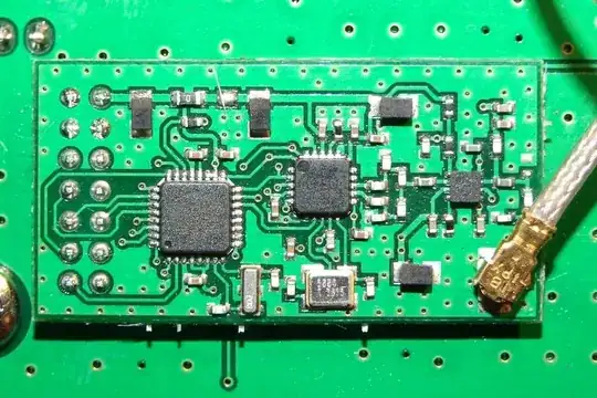
I have a 3"x3" 4-layer PCB where my stack up is:
Signal 1
Ground
5v Power
Signal 2
My Signal 1 layer has a few traces that carry 500 MHz on them, some high resolution ADCs, and microcontroller/usb circuitry. I have SMA connectors that are carrying the 500 MHz on to the board. Currently this will just be "open air" sitting on a test bench, but long term into will end up in a case in which everything will be contained internally.
My Signal 2 layer has almost nothing on it, specifically it has the following:
- MCLR from programmer connector that is 0.1" long
- SPI Data and Clock line that are both about 0.1" long
- Negative voltage (for powering 2 op-amps) trace that is about 2" long
I feel like it is somewhat of a waste to have so much unused PCB. I am considering the following options:
- Fill the layer with my negative voltage rail
- Fill the layer with ground
- Leave the layer empty
Is there any benefit of one of the options over the other? What is usually done in these situations?
Some Additional Details
The system will be pulling a peak of 300 mA off of the 5v rail. While the -5v rail will only have about 2 mA load.