I'm back to diagnosing power supply failures, in an LLC resonant SMPS based on the L6598, from a 400 V PFC supply with ostensibly 400 W output. I'm new to SMPS, and learning this all as I go, and the manufacturers don't know what they're doing, either; they just copied the design and modified it for more bigger power. The circuit is basically like Figure 3 in AN-9425, but the OPOUT overcurrent detection triggers EN1 (latched) instead of EN2 (soft-start reset).
The failures happen during overload, when the supply is making audible screaming noises and the output voltage has dropped (because it's switching below the resonant frequency, right?) Sometimes it can withstand a prolonged overload (without triggering EN1), sometimes it can't. Sudden transient overloads are usually what kill it. Not sure if it's a progressive damage thing that eventually results in failure or a random spike that exceeds a limit. Theoretically, it should handle overloads by shutting off momentarily or otherwise protecting itself, not by exploding.
Theoretically, I could change the overcurrent protection so that it detects when it's being overloaded and triggers the soft-start EN2 protection mode, shifting the frequency up high to drop the output voltage instead of dropping below the resonant point. I tried modifying the circuit to match the app notes so OPOUT drives EN2, but that just made it blow up even more quickly when I overloaded it.
The L6598 controller IC always fails, the STW20NM60 MOSFETs fail sometimes (high side short across all pins, low side short from D to S), so I think the IC is failing first and taking the MOSFETs with it? The MOSFETs don't have built-in gate protection, so I added Zeners externally and they haven't failed since (yet). New ICs measure open circuit from any pin to any other, but after I remove a failed IC from circuit, some of the high pins will have kΩ between them (12 Vsupply, 14 Vout, 15 high side driver, 16 bootstrap cap).
Today I was manually triggering the EN2 pin, which worked fine at low loads, changing to a high switching frequency and output voltage dropping. At about 200 W out, it worked fine when I enabled EN2, but when I let go of EN2 it would shut down (overcurrent protection triggering EN1 is the only way I know of) and then another time failed. After it failed, the low side driver would still switch at fmin (no output voltage to drive the feedback loop), but the high side driver just had spikes and weird shapes on it, not a square wave. The MOSFETs measure normally with an ohmmeter and didn't explode. So some kind of spike is killing the high side section of the IC and I need to prevent that.
I certainly don't see any pins going higher than the 618 V absolute max rating. I do see tiny spikes going down to -3 V before the rising edge on Vout and VHVG, which are rated for -1 V. I don't know if that really matters. I'm not sure about the ratings for Vout or VHVG, or how I would even measure those (differential probe?), or what conditions would cause them to go beyond the stated limits. They seem to track each other, as would be expected if the high side driver is floating relative to Vout.
What am I missing?
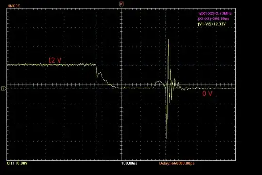
Update:
There are huge bursts of oscillation(?) ±25 V on the gate driver while overloading, 100s of ns after the rising or falling edges, which coincide with the audible noise. These could easily break through the gates and destroy the FETs, so they are the prime suspect. They originally had ferrite beads on all the FET pins, which did not prevent this, nor does removing them. I've added Zener protection to the gates, though, which should prevent them from being destructive, but I'd like the eliminate the bursts themselves first.