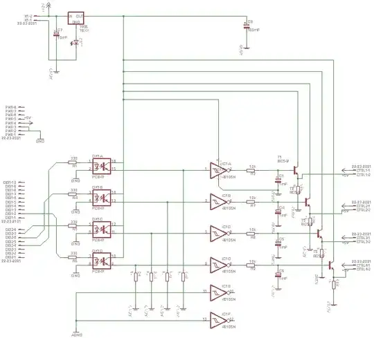
I'm designing an Arduino shield to manage the control signal that reaches 4 CCFL inverters.
As part of the circuit design, I've decided to use optocouplers to isolate the Arduino's microcontroller from the rest of the circuit. If I'm right, in order to get the proper galvanic isolation I need to separate on one hand the Arduino's GND and on the other hand the power supply's AGND which feeds the part of the circuit (through 7806) aimed to generate that specific control signal.
Am using Eagle CAD software and I've used different GND symbols to separate the different grounds coexisting in my circuit, but when switching to PCB design all of them seem to be together joined in the same net.
These situation makes me wonder several questions:
• Am I right when I'm trying to separate grounds in order to get galvanic isolation?.
• I've found this post that seems to talk about a similar question: How do I facilitate keeping multiple grounds, (i.e. AGND, DGND, etc...) separated in the layout when using Eagle? but I'm not sure if the solution proposed really fixes my problem, because if I understood correctly they end up joining GNDs in one point to have a global ground reference.
• If I am right, which is the best way to manage different GNDs in the same circuit in Eagle schematic design?
Here it is the schematic I'm working on:
Thanks for your help!