3

i just want to get the idea for the input voltage protection for a fully differential ADC.

The analogue voltage inputs supposed to be 0-5v, but someone being careless could plug a higher voltage (up to probably around 20v) by accident and blow the ADC.

I have seen zener regulation/clamp circuits, but upon trying them realized that they of course produce a voltage drop. The voltage needs to be unaltered from the one the user puts in, so this does not work for me.

So, what I need is a way to protect my ADC inputs from over voltage as high as ~20VDC or more but still be able to accurately read a 0-5V nominal analogue signal without altering the voltage reading.

and my power supply for the board is 5V, so i only want to limit the input signal to 0-5V. yeah, of course the Voltage must be above 0.

besides, i have only found one overvoltage/undervoltage from TI , It is TPS2400 , but the range of the protection voltage is 3 to 6.9. it's not suitable for me.

so , is there any programmable VOP and UOP chips that i can use? the ADC that i use is ADS5272enter link description here

Any suggestions? Let me know! Thanks a bunch in advance!

i posted the Zener diode grafic enter image description here 
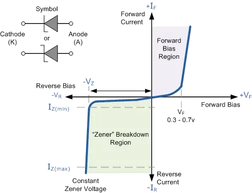
see that , from -Vz to Vf it is not linear, and i thing it must have an effect on the input singal for ADC

napon
  • 39
  • 1
  • 4
  • What is the input impedance of your ADC? What is the output impedance of whatever's driving the ADC? What temperature range does your system need to operate over? – The Photon May 12 '15 at 16:51
  • 1
    You cannot have high accuracy up to 5V and limit the voltage to 5V. There needs to be a **difference** between the maximum signal level and the maximum clamping level, if only for tolerances. And an accuracy spec or at least how many bits the ADC is.. something... – Spehro Pefhany May 12 '15 at 17:11
  • if it's a once-off accident protection you want, why not use an overvoltage (set to trip at 6V for example) clamp circuit or FET based switch array which basically open-circuits the inputs from the ADC pins? – KyranF May 12 '15 at 17:25
  • I imagine a dual or quad op-amp set up as comparators to trip at 6V and turn off some high-side PFETs (using low Rds_on as possible, to reduce effect on your ADC circuit) would be enough. You could even use a good old flip-flop latch which only a power-cycle can reset – KyranF May 12 '15 at 17:27
  • @KyranF thanks for your replay. this is the idea that i already found, but if the input of Op amp is beyond the voltage supply of opamp(5 V), the Opamp will not work propertly and blow, isn't it? so i think we can not limit the voltage using Opamp。 – napon May 12 '15 at 17:50
  • @napon you don't limit the voltage with an op-amp, you detect that the voltage has gone above limits using voltage divider and comparator reference voltage - the output will control a set of P channel MOSFETs, which literally disconnect the ADC from the input, to protect it. – KyranF May 12 '15 at 17:54
  • The ADC that you linked to has an absolute maximum supply voltage of 3.8 V, and a recommended operating maximum of 3.6 V. You cannot have an input voltage range of 0 - 5 V with that ADC. – The Photon May 12 '15 at 17:54
  • @ThePhoton agreed. There is some confusion here, OP needs to read up about protecting ADC inputs, and read the datasheet more (And comprehend it) – KyranF May 12 '15 at 18:04
  • @napon, on zeners, see the linked question. You hook the zener up so that it is normally reverse-biased, and the region of the i-v curve around \$V_f\$ doesn't affect the operation. – The Photon May 12 '15 at 18:15
  • If you want to ask a question about how zeners work, first please search to see if it's been asked before. If not, then please post a new question. – The Photon May 12 '15 at 18:16

1 Answers1

3

In terms of behaviour of the input protection circuit, you have three choices:

  1. Clamp - voltage goes too high and is held at the clamp voltage, which is equal to or less than the max voltage input for the ADC.

  2. Some kind of limiter design which uses an amplifier and reduces the gain of the amplifier to ensure that its output does not exceed the ADC input voltage, as the input voltage increases.

  3. Input disconnection circuit. This option has been covered by another poster so I won't cover it here.

The problem with option 2 is that the signal that you want to measure is passing through the amplifier and therefore being subjected to modification by the varying gain.

In theory, you could use option 2 if you activated the variable gain facility when the signal of interest got very close to the max input of the ADC, so that for most of the input voltage range of the ADC, the gain of the variable gain amp would be \$1 (V_{out} = V_{in})\$.

You'd have to use a comparator circuit to trigger the variable gain feature, and the gain of an op-amp circuit (a simple inverting op-amp is: gain = \$-R_f/R_{in}\$), so you'd have to have a FET or other transistor in the feedback path of the operational amplifier to allow the value of \$R_f\$ (expressed in ohms) to change.

For example: design a comparator using an op-amp (easy enough) to trigger at say, 4.9 volts the FET in the feedback path of an amplifier switch different values of resistance into the feedback path of the op-amp, so from 0 - 4.9 volts, the gain of the amplifier is 1 and the input signal passes unchanged to the ADC input.

In theory this can be done, but to be honest, it's getting complicated.

I reckon you'd need 3 operational amplifiers, one for the comparator, one for the variable gain amplifier, and possibly a further one to invert the signal so it's the right way up for input into the ADC. This kind of approach is used in the audio business to limit the output level so that as an input audio level goes high, the gain of the amplifier circuit reduces to ensure the output doesn't go too high.

Option 1: Clamp

Diodes and Zeners are often used to protect the logic inputs on digital chips from the high voltage static electricity.

I'm not sure what circuits you are looking at that you think modify the input voltage. A Zener diode is just a diode that's been designed to break down at low voltage (when a diode is reverse-biased).

You might need a resistor in series with the Zener to limit the current, but both the resistor and Zener are arranged in parallel across the input to the ADC.

Zeners come in standard voltages, so you might find a Zener that breaks down at say 4.6 volts, a bit less than 5 volts.

When the input to the ADC is less than 4.6 volts, the zener is not operational. Its resistance is very high; almost no current is drawn.

Vin---------------> Vadc...... ADC input
      |
      R
      | ------ Vz
      |
      Z
      |
---------------- OV

Under this circumstance \$V_{adc} = V_{in}\$, Z has a very high resistance. (Which puzzles me as to why you think such a circuit affects the \$V_{in}\$, the input signal. If you're dealing with high frequencies, then capacitance of the Zener might come into play and affect the signal, but I'm assuming you're not dealing with signals that high in frequency.)

Now when \$V_{in}\$ goes too high, say 4.7 volts (you need 4.6 across the Zener, and say allow a bit of voltage across the resistor), the Zener will break down and conduct, ensuring that only 4.6 volts is across the Zener, regardless of how high the \$V_{in}\$ goes. \$V_{in}\$ goes to 5 volts and higher, but the Zener is conducting and holding \$V_{out}\$ at 4.6~4.7.

The Zener is conducting, so current is now passing through it, but the resistor R limits that current to prevent a) burn out of the device and b) prevent whatever is supplying the signal \$V_{in}\$, from burning out its output stage.

When the Zener is conducting, you will need a bit of current through it, its operating current in order for it to break down at its specified breakdown voltage. Some Zeners require a few milliamps, but lower operating current Zeners can be found that operate at much lower current. Good selection of Zener and correct calculation of the R value are important to ensure that a) the Zener breaks down at the correct voltage and not a higher voltage (because the operating current is too low), b) you limit the current to a safe value for both the Zener and output of the previous stage that is supplying \$V_{in}\$.

I think you need to look at the Zener circuits again. Can you explain why you think there's a voltage loss - I understand accuracy of the \$V_{in}\$ to the ADC is important.

JYelton
  • 32,302
  • 33
  • 134
  • 249
Dean
  • 838
  • 4
  • 7
  • In addition to zener clamps (or schottkys to VCC and GND) to ground from each ADC pin, I think a series resistor from the input to the ADC terminals would go a long way to making the ADC pins more resistant to abuse – KyranF May 12 '15 at 17:42
  • The series resistor approach would cause a voltage drop across it and render the volate into the ADC to be inaccurate, which he doesn't want. – Dean May 12 '15 at 17:48
  • no, series into the ADC pins, not series to ground/with load – KyranF May 12 '15 at 17:54
  • See ThePhoton's answer here http://electronics.stackexchange.com/questions/35807/how-would-i-design-a-protection-clipper-circuit-for-adc-input – KyranF May 12 '15 at 17:56
  • 1
    Note that OP is totally confused about what he's doing. His ADC has 3.3 V supply, has differential input, and the datsheet recommends at least 20 ohms in series with the inputs. – The Photon May 12 '15 at 17:59
  • @Dean thank you very much for the suggestions that u gave! – napon May 12 '15 at 17:59
  • @Dean, but according to the work area of Zenner circuit, it is nolinear, so i think the input voltage for ADC must be get affected – napon May 12 '15 at 18:00
  • @napon, the nonlinearity is **why** the zener doesn't affect the adc input until it's zener voltage is exceeded. – The Photon May 12 '15 at 18:07
  • @Photon, thanks a lot for your answer ! but before the voltage reaches the Zener Voltage, the signal voltag consists a part of voltag drop on Zenner, and it is not linear, so the input signal will also be nonlinear, it causes troubles for the accuratity – napon May 12 '15 at 18:20
  • @napon no, the zener does NOT conduct until the voltage exceeds the breakdown voltage, THEN it conducts, and THEN it will not matter because you've already gone past the rated input voltage for your ADC. Get a Zener which turns on/has effect after the working range of your ADC. 5V ADC, get a 5.1V zener. 3.3V ADC, get a 3.7V Zener or something. – KyranF May 12 '15 at 18:21
  • @napon, there are no ideal devices in the real world. If your source's impedance is low enough then it will be able to provide enough current to minimize the error due to the leakage through the zener. If your source's impedance is high, then use the clamp diodes to power and ground solution, also shown in the answers to the linked question. – The Photon May 12 '15 at 18:22
  • Note that the clamp diode solution also has a small leakage current. There is no free lunch. – The Photon May 12 '15 at 18:22
  • @KyranF A 5.1V zener will be conducting LOTS of current at 5V. Like [this](http://4.bp.blogspot.com/_HJ-P1iIFXtk/TIXlTNpkkTI/AAAAAAAAAe4/GN3QFWbU3EI/s1600/RS+5_1V+Zener+Characteristics.png) one that is conducting about 10mA. Even if it's an 8-bit converter that's a lot of error. 3.7V zeners are much, much worse. If his input can take 6V and the signal is restricted to 2.5V, a 5.1V zener might be acceptable. – Spehro Pefhany May 12 '15 at 20:54
  • @SpehroPefhany if the system is 5V max signal, then maybe a 5.6V zener is better. Either way I personally would avoid zeners and just go for dual schottky clamps and series resistor to limit current – KyranF May 12 '15 at 21:25
  • sorry for one more question. i planned to use a schokkty clamp circuit. do you know which IC is property for my work, i think i need less voltag drop. – napon May 13 '15 at 08:15
  • @ThePhoton thanks a lot for the help. now i was thinking if a stable 20V input voltage will burn the schottky diode.. and i saw your answers in another question, there should be a resister to limit the current thus to protect the diode. but could u tell me more detail, where to put the 15k resister? – napon May 13 '15 at 13:03
  • @napon, nobody's mentioned a 15k resistor before, so just leave it in your parts drawer. – The Photon May 13 '15 at 16:36
  • Let me explain what a zener diode is and why in theory it shouldn't have any effect on the signal of interest. A conventional diode has a reverse breakdown voltage of say 100 volt & operates in forward bias. A zener is a diode which is designed to have a low break down voltage, equal to the zener voltage, say 5.6V and the diode operates in reverse bias so that when the voltage across it is high enough it breaks down at the stated voltage. Diodes electrical characteristics have 2 parts: exponential I-V relationship in forward bias, in reverse bias, zero current flow until... – Dean May 14 '15 at 12:52
  • in reverse bias the diode has a very high resistance,so almost no current flows (only the reverse saturation current flows), until the voltage across it is is large enough in value (negatively biased) that the diode breaks down and the resistance drops massively and close to zero. If you examine the IV curve of a diode you can see this. A zener should display very similar characteristics to a reverse biased diode, just that the break down voltage is much lower. So a zener shouldn't conduct until the break down voltage is reached – Dean May 14 '15 at 12:58
  • As the voltage across the zener increases, its resistance should be very high and therefore should not affect what it's connected to (if connected in parallel), when the voltage across the zener reaches the breakdown voltage, then its resistance drops to close to zero (or low anyway). But ideally, go seek out the IV curve for the zener of your choice and take some measurements from it to be safe. – Dean May 14 '15 at 13:04