22

Can a TO-220 without a heatsink dissipate 1W in still air?

Or, a different way of asking the question is: Assuming an ambient temperature of 25C, how can I go about calculating the maximum power I can dissipate on a TO-220 packaged MOSFET? The MOSFET is a FDP047N10 if that helps. It will be handling about 12.5A of continuous current (ie, no switching).

I would also like to understand the difference in power dissipation of a MOSFET which is continuously ON, vs a MOSFET that switches at 100KHz (50% duty cycle ON).

One final question: If I parallel two MOSFETs to reduce the power dissipation per FET, is there anything I can do to make sure (or increase the probability) that both will supply equal amounts of power?

stevenvh
  • 145,145
  • 21
  • 455
  • 667
SomethingBetter
  • 2,260
  • 7
  • 26
  • 33
  • 9
    I added a link to the part's datasheet. We're trying to make users aware of the importance of this, especially for less common parts, so that others don't have to go searching for it and that everybody is sure to be talking about the same thing. Just trying to cultivate good habits. – stevenvh Jul 15 '11 at 15:29

8 Answers8

18

This is simple: do the math. Look at the datasheet. There should be a thermal resistance spec that tells you how many degC difference there will be between the die and ambient air per Watt. Then add that to your worst case ambient temperature and compare to the maximum allowed die temperature.

For most transistors and ICs, a TO-220 case will get hot at 1W, but generally stay within operating range. At 1/2 W I wouldn't worry about it. At 1W I'd check the datasheet and do the calculation but it will probably be OK.

One wrinkle: The datasheet may only tell you die to case thermal resistance. You then have to add the thermal resistance from the case to ambient, which will be much higher. Fortunately that's mostly a function of the TO-220 case, not the transistor, so you should be able to find a generic figure for that. Good datasheets give you both thermal resistance figures.

Added:

I hadn't followed the datasheet link earlier, but now I see that everything you need is well specified in there. The thermal resistance from die to ambient is 62.5 C/W, and the maximum die operating temperature is 175C. You said your ambient temperature is 25C. Adding the rise from there to the die at 1W yields 88C. That's 87C below the maximum operating temperature, so the answer is very clearly YES, your transistor will be fine at 1W in 25C free air.

Olin Lathrop
  • 310,974
  • 36
  • 428
  • 915
  • 11
    "*This is simple: do the math*", isn't that the answer to just *any* question here? :-) – stevenvh Jul 15 '11 at 15:33
  • 1
    @Olin: About the thermal resistance ratings: For an SMT MOSFET such as BSC060N10NS3 (digikey link: http://search.digikey.com/scripts/DkSearch/dksus.dll?Detail&name=BSC060N10NS3%20GCT-ND), is the junction to ambient rating given only for the heat dissipation through the pad underneath the device? Or, to put the question another way, if I mount a heatsink on top of the SMD mosfet, are the thermal dissipation equations governed by the same thermal resistance data in the datasheet? – SomethingBetter Jul 15 '11 at 16:01
  • 1
    @Something: Datasheets don't usually spell this out, so I'd take it to mean to whatever surface to you attache a heat sink to. This expoxy enslosing the die would *not* qualify for that. – Olin Lathrop Jul 15 '11 at 19:51
  • 1
    @SomethingBetter - You'll have better cooling, because, despite adding another thermal resistance to the heatsink, this will be *much* smaller than the difference in thermal resistance to ambient. Remember: conduction is low thermal resistance, convection is high, so it's worthwhile focussing on the latter, and a big heatsink will do much better than a small component package. – stevenvh Jul 16 '11 at 13:13
  • 1
    @stevenh: Yes, but if I can't quantify it, it is hard to design for it. – SomethingBetter Jul 17 '11 at 17:50
  • BTW, looks like IR DirectFET packages can be cooled with a top heatsink : http://www.irf.com/product-info/directfet/ – SomethingBetter Jul 17 '11 at 21:17
17

Answering your second question:

A switching MOSFET will have two types of losses; conduction and switching. Conduction loss is the usual \$I_D^2 \times R_{DS(on)}\$ loss. If you control the MOSFET so that it's on with 50% duty cycle, the conduction loss is 50% of the DC (always-on) loss.

Switching losses include the amount of energy needed to control the gate and losses in the device as it transitions from the on-state to the off-state. When you're turning on a MOSFET, there is an interval where \$I_D\$ starts to flow and the \$V_{DS}\$ voltage is still at its maximum. \$V_{DS}\$ falls as the MOSFET channel saturates. The power consumed during this time is called turn-on loss. Similarly, at turn-off, there's an interval where \$V_{DS}\$ rises before \$I_D\$ starts falling, which (not surprisingly) is called turn-off loss.

You must consider the turn-on and turn-off losses when you're talking about 100kHz operation. Most likely you will see less power than the DC condition, but you won't be saving 50%.

Answering your third question:

MOSFET \$R_{DS(on)}\$ has a positive temperature coefficient - the warmer it gets, the higher the \$R_{DS(on)}\$ gets. If you connect two MOSFETs in parallel with similar characteristics (i.e. the same part number from the same manufacturer), drive them identically, and don't have huge asymmetry in your PCB layout, the MOSFETs will indeed share current quite nicely. Always make sure each MOSFET has an independent resistor in series with each gate (never parallel gates without resistors) as gates tied directly together can weirdly interact with each other - even a few ohms is better than nothing.

Adam Lawrence
  • 32,921
  • 3
  • 58
  • 110
11

Answering your first question:

let's start with the power consumption. Datasheet says 4.7m\$\Omega\$ maximum at 75A, and at 12.5A this will be less, so that's a safe value. Then \$P = I_D^2 \times R_{DS(ON)} = 12.5^2 \times 4.7m\Omega = 735mW\$. Add some extra safety and 1W is a good value.
What a part can dissipate depends on

  1. the amount of energy generated,
  2. how easily the energy can be drained to the environment

(The first factor says "energy", and not "power", because it's energy that causes temperature rises. But in our calculations we assume steady state, and can divide everything by time so that we can work with power instead of energy.)

We know the power, that's 1W. How easily the energy can be drained is expressed in thermal resistance (in K/W). This thermal resistance is the sum of a few different thermal resistances which you normally (should) find in the datasheet: there's the junction-to-case resistance and the case-to-ambient resistance. The former is very low, because the heat transfer is through conduction, while the latter is a much higher value because here the heat transfer is through convection. Like Olin says the latter is a property of the case type (TO-220), so maybe we won't find it in the datasheet. But we're in luck, the datasheet gives us the total thermal resistance, junction-to-ambient: 62.5 K/W. That means that at a 1W dissipation the junction temperature will be 62.5 K (or °C) higher than the environment. If the temperature in the enclosure is 25°C (that's rather low!), then the junction temperature will be 87.5°C. That's much less than the 125°C which is often assumed as a maximum temperature for silicon, so we're safe. The case temperature will be almost the same as the junction, so the MOSFET will be HOT, too hot to touch.


Note: this web page lists the case-to-ambient thermal resistance for different packages.

stevenvh
  • 145,145
  • 21
  • 455
  • 667
6

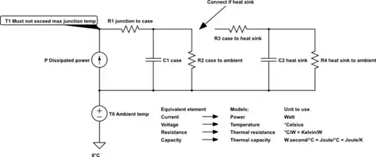
As a complement to the other answers, here is an equivalent circuit with which you should be able to work out whether your component can handle the dissipated power, be it a TO-220 or any other package, with or without a heat sink.

schematic

simulate this circuit – Schematic created using CircuitLab

If the voltage source is bothering you when solving for the junction temperature ("voltage"), you can remove it and work on the temperature elevation with respect to the ambient temperature (GND is now Ambient temperature/potential).

  • R1, R2 and C1 come from the component datasheet
  • R3 comes from the datasheet of the thermal paste used if any, or from charts of thermal resistance VS contact pressure (depends on contact area) for the materials in contact
  • R4 and C2 come from the heat sink datasheet, R4 should depend on the airflow.

Generally, "case" means tab if there is one (the actual case otherwise), but otherwise you should be able to tweak the equivalent circuit accordingly - just think about the resistors as paths for the heat, and you get the temperature of an element from its voltage.

For steady state, assume the thermal capacitors are removed (fully "charged"/heated up). For example, without heat sink:

$$T_1=T_0+(R_1+R_2)P=30+62.5*1=92.5°C<\frac{150°C}{1.5}$$

When the dissipated power is switched fast compared to the thermal time constants, you generally have to multiply the specific capacitance that the manufacturers may give (rule of thumb is 3 (W.s)/(K.kg)) with the associated mass to get the capacities, and deal with usual RC charges.

Note that the ambient temperature around the component may be much higher than the ambient temperature around you, if the air is not circulating and/or if it is enclosed. For this reason, and because all the values are generally not very accurate, be critical about T0 and take at least a safety factor or 1.5 (as above) or preferrably 2 on T1.

Finally, you might want to consider looking at the plots VS junction temperature on the component datasheet and changing the max temperature for a lower one, as an OK-ish temperature might ruin your circuit's performance, still. In particular, temperature cycling reduces your component's lifetime - a rule of thumb is the lifetime halves for every 10°C increment.

Mister Mystère
  • 9,477
  • 6
  • 51
  • 82
2

The "die to ambient" thermal resistance means mounted on an infinite heatsink, or, commonly, a 1 inch square copper pcb, or some similar test specified by the manufacturer. When the device is mounted like that, the "ambient" temperature is the temperature of the heat sink. If the device is not mounted like that, the "ambient" for the device will be the temperature of the hot air surrounding the device, not the 25C of some air somewhere further away.

The thermal resistivity of still air is around 0.1 - 0.2 K/W, per square metre, and the area of a TO-220 package is around 300 mm2, so a first guess at the ambient-to-environment thermal resistance would be around 500C/W. This agrees with the kind of numbers available on the internet: TI suggests that the thermal resistance from a 1 cm square to air due to natural convection is 1000 K/W.AN-2020 Thermal Design by Insite, not Hindsight

With the environmental temperature around 25C, Thermal resistance around 500 case-to-environment, around 50 junction to case, and maximum junction temperature 150C, permissible power is (150-25)/550 W, or, very roughly,

around 200 mW.

david
  • 4,364
  • 15
  • 30
  • 1
    From my practical experience, 1W is a limit which I push sometimes on a TO220 case, usually for temporary work and for tests. It is a limit at which the steady state case temp approach 100'C; I am not using it for final products because i prefer to work for fiability; but for tests is okay – addysoftware Jan 03 '18 at 15:01
2

According to wiki formula and constant for TO-220 junction-to-air thermal to ambient equal 62.5 degree per watt. When your junction is at 125C-70C ambient (worst case)/62.5 = 55/62.5 = 880 milliwatt.

That the limit say for automotive applications.

So answer is No. Even if you are able to maintain limit of 125C (ouch).

You also asking if it is applicable to FETs. It is even more questionable for FETs, because they have a thermal runaway mode, when with inrease of junction temperature their electrical curves tend to aim even more power dissipation. So you can not maintain the limit. Paralleling FETs will not degrade runaway and they will self-balance the load, but small differences in devices will cause inrush current induced ringing of gate voltages (you have large current spikes next to high impedance pins), so it can oscillate and degrade thermally. (Edit: as Madman commented: When you switch at zero-cross time, say in synchronous rectifier, you can ignore this aspect).

So final answer is No and No.

My conservative estimation is 880 divide by 3 = about 300 mW, to keep safety margin of 200% excess of wattage.

  • 2
    It is extremely common in switching power to parallel MOSFETs, so I must disagree with your conclusion about paralleling being a bad idea. – Adam Lawrence Jul 15 '11 at 15:41
  • @Madman Did you follow the part about ringing, oscillation, when uneven FETs open/close at slightly different time ? With some sloppiness in layout, you can easily end with unexpected 10MHz high power oscillator –  Jul 15 '11 at 15:49
  • 2
    It's not uncommon in the power supplies I work on to have 12-16 MOSFETs in parallel (synchronous rectification) and 2 in parallel in the PFC preregulator. Therefore, I maintain that your "final answer" of "No" when talking about paralleling MOSFETs is one which I must disagree with. – Adam Lawrence Jul 15 '11 at 15:54
  • Well what applies to XX KHz is much less of concern at 50/60Hz. I bet your synchronous rectifier drive has a closely watched dV/dt curve (in other words filtered to have no harmonics higher than X MHz). So parts can have about few hundred ns lag relative each to other. Anyway +1 for pointing it out, that one can ignore this limitation sometimes. –  Jul 15 '11 at 16:00
  • 3
    Thanks. My synchronous rectifiers are operating at 170kHz with commercial driver ICs, FWIW. – Adam Lawrence Jul 15 '11 at 16:19
  • 1
    If the voltage across a MOSFET is fixed, I believe normal behavior would be to pass through less current as it gets hot, thereby reducing the amount of heat generated. The reduction might not be sufficient to prevent device destruction, but I would not regard the failure of a MOSFET in a voltage-limited situation as thermal runaway. BJT's exhibit the opposite behavior, letting more current through as they get hot. At a fixed voltage, that would translate into increased power and thermal runaway. In current-limited applications, MOSFETs would exhibit runaway and BJT's not. – supercat Jul 15 '11 at 17:47
  • @supercat. You brought an inapplicable model with fixed voltage. It is fixed current. The mode of interest is Rds on with specified current, not voltage. So P=RI2, where I comes from current source with internal resistance of "load", which is much higher than Rds on. For example 24V, 20A, 0.8Ohm motor and 0.02 Ohm FET –  Jul 15 '11 at 17:53
  • @Rocket Surgeon: If a MOSFET is trying driving a fixed resistive load from a fixed supply voltage, power dissipation in the MOSFET will be maximized when its voltage drop is half the supply voltage. If the voltage drop is more than half the supply voltage, factors which cause the MOSFET to let through less current or increase its voltage drop will cause a reduction in current more than proportionate to the increase in voltage, thus causing a reduction in power dissipation. – supercat Jul 15 '11 at 19:39
  • @Rocket Surgeon: If the fixed resistive load is sufficiently small that the MOSFET simply can't conduct well enough to get its voltage drop below half-rail (a common situation if one's load gets shorted out), then any reductions in MOSFET current will yield reductions in heat dissipation. – supercat Jul 15 '11 at 19:42
  • 1
    Your answer is inconsistant with itself. According to the datasheet the op linked to and your own figures, the thermal resistance from die to ambient is 63 C/W. The OP specified ambient to be 25C and dissipation to be 1W, so that puts the die temperature at 25C + 63C = 88C. That's 87C below the maximum die operating temperature of 175C. That represents almost another 1.4W of margin. Sounds like a "yes" to me. – Olin Lathrop Jul 15 '11 at 19:48
  • @Olin. Agree for 25C. No arguing with arithmetics. I picked 70C is the value for most liberal use case for commercial temperature range (not industrial, not military). –  Jul 15 '11 at 20:38
1

david has basicley said that the mosfet will go bang +1 .Some other reasons would be the nasty positive temp co of on resistance which does not work in your favour when the device current is fixed .In fact like most fets it can easily double as it gets hot so your 1watt is now 2 watts .The high input capacitance will cause power to be wasted in the internal gate resistance if your gate driver is fast .This gate power is significant and should be factored in .If you drive slow your switching losses will go up especially if you are hard switching so you cant slow the gate up much .If your DS voltage is reasonably high the miller effect starts to amplify the drain gate capacitance .This extra capacitance adds to the already large gate source capacitance making things even worse.If all this is not enough consider diode recovery at turn on .

Autistic
  • 14,235
  • 2
  • 27
  • 65
-1

The question I did not see but was expected to be answered too: what size of heatsink is needed then.

This link may be useful for answering that (It boils down to your cooling situation and temperature difference)

https://celsiainc.com/resources/calculators/heat-sink-size-calculator/

nomail
  • 1
  • 2
    Welcome to EE.SE. Note that link-only answers are of little use when the link dies. Your answer should give enough detail that it stands on its own. Please take the [Tour] to learn more about how the site works and its policies. – Transistor Oct 21 '20 at 17:50