3

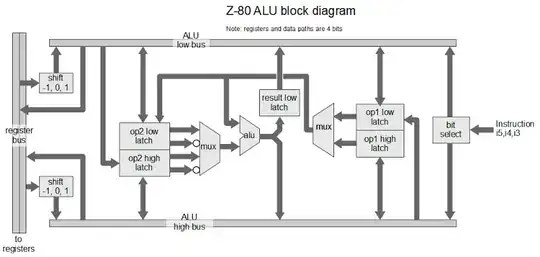
Z80 was a popular 8-bit processor with a 4-bit ALU.

Z80 ALU

Implementing a zero flag for a register should be straight forward, it would be a logical NOR of all the bits on the register.

Gigantic NOR

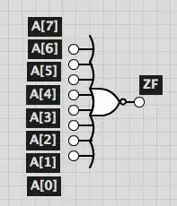
Something like that would work for a small number of inputs. As for a 64-bit processor you cannot make one gigantic NOR gate with 64 inputs. The fan-in would be too high. Too many transistors would be in series.

So, I can see some other options (non-exhaustive list).

  • The zero flag could be generated directly from the 8-bit result using 2 level logic.

two level logic two level logic

  • The zero flag could be generated directly from the 8-bit result using 3 level logic.

three level logic

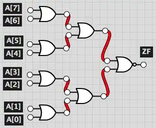
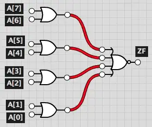
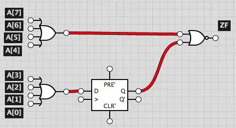
  • The zero flag could be generated from each nibble and then put together, like if there was a "half"-zero flag. The result for the lower would be saved using a flip-flop while waiting for the high nibble result to be calculated.

Nibble

Ken Shirriff wrote a nice article about reverse engineering the Z80 ALU. However when it comes to the zero flag he states:

Not shown in the block diagram are the simple circuits to compute parity, test for zero, and check if a 4-bit value is less than 10. These values are used to set the condition flags.

So, although they are simple circuits I would like to know exactly how they were implemented and if they used any of the implementations proposed above or something else completely different.

There is a related question where they talk about zero flag implementation in general terms.

GabrielOshiro
  • 211
  • 4
  • 11
  • I believe modern CPUs are designed using software that is capable of automatically generating multiple stages if fan-in is too high. – Simon Richter May 28 '15 at 18:14

3 Answers3

3

I have got a response from Mr Shirriff himself that not only answers my question but also gives more details on the rest of the flag circuitry.

That's a good question. The zero flag is generated in the ALU by NOR of all 8 bits: the 4 bits that were just generated by the ALU, and the 4 bits that are latched in the ALU from the previous half-operation.

Carry on the other hand is much more complicated. The 4-bit operation generates the half carry, which is latched. There's a bunch of logic to handle addition vs subtraction, shifts, etc. Then the next 4-bit operation generates the fully carry.

Parity is generated by exclusive-or of the first 4 bits. That result is then fed into the exclusive or of the next 4 bits to generate the final parity.

Ken

GabrielOshiro
  • 211
  • 4
  • 11
1

When using CMOS logic, NAND and NOR gates with a high degree of fan-in are problematic because while one side of the gate will have lots of transistors in parallel (no particular problem with 8-wide fan-in, and probably not even for 64-wide fan-in), the other side will have lots of transistors in series (yielding propagation time proportional to the square of the number of series transistors once things get much beyond 3-4). The original Z80, however, was not implemented using CMOS logic, but rather NMOS logic.

When using NMOS logic, an 8-input NOR gate would generally have eight transistors trying to conditionally pull a signal down and a passive pull-up trying to unconditionally (but weakly) pull it up. Dynamic NMOS logic (used in the 6502--not sure about the Z80) could make things a little more power-efficient, at the cost of imposing a minimum operating speed, by having a signal unconditionally pulled up during one half of a clock cycle and then conditionally pulled low during the other half; parasitic capacitance effects are sufficient to ensure that if nothing pulls the signal low during the second half of the cycle, it will stay at a valid high level for at least 5us (half a clock period at the minimum allowable speed). In either case, using an 8-input NOR gate is no worse than two four-input NOR gates, even if the latter wouldn't require additional circuitry to yield the Z flag value.

BTW, the NMOS 6502 could perform binary-coded decimal arithmetic at the same speed as binary arithmetic; the CMOS version of the 6502 is slower (it takes an extra cycle) and other processors generally require separate "binary add" and "cleanup" steps. I suspect that the ability to have complicated pull-down networks without having to have complementary pull-up networks made that possible, though the 6502's BCD arithmetic circuitry is sufficiently complex I never understood it.

supercat
  • 45,939
  • 2
  • 84
  • 143
0

It doesn't really matter so long as the answer is reliably ready in time for the next clock edge. I'm not sure you can expect a definitive answer- the original designers are probably well past their best-before dates by now- unless a transistor-level description has been released.

Here's some insight into transistor-level design in the Z80.

Actually, for a simple 8-input NOR gate, there would be 8 transistors in parallel (and none in series, save for the load) in the case of the original ca. 1976 Zilog NMOS Z80. I suspect that's exactly how they would have done it.

Spehro Pefhany
  • 376,485
  • 21
  • 320
  • 842