8

This is Figure 9-3(b) from Motchenbacher - Low-Noise Electronic System Design, so I would expect it to work, but I don't understand it:

The addition of a discrete common-source stage at the input can offer lower noise. Overall negative feedback to the source of a common-source input stage, as shown in Fig. 9-3b, raises the amplifier's input impedance.

enter image description here

It seems like positive feedback to me:

  1. Decrease in Vin →
  2. Decrease in Vgs →
  3. Decrease in Id →
  4. Increase in Vd → (like a common-source amplifier so far)
  5. Increase in Vo →
  6. Increase in Vs →
  7. Decrease in Vgs →
  8. Decrease in Id →
  9. ...

Am I missing something?

For comparison, here's another circuit that is similar, but looks like negative feedback, and has actually been built and works:

enter image description here

Edit:

So that picture is from the 1993 edition. I got my paper 1973 edition off the shelf (no Ctrl+F!), and the equivalent figure is 7-3(b), but with a BJT and the op-amp pins reversed:

Overall negative feedback to the emitter of a common-emitter input stage raises the amplifier input impedance.

BJT connected to op-amp

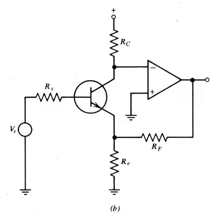
This makes more sense to me. If the collector voltage tries to rise, the op-amp drops the emitter voltage to pull it back down and keep the collector at 0 V. So I'm thinking the first diagram is just a mistake.

endolith
  • 28,494
  • 23
  • 117
  • 181
  • 1
    I think the top circuit will work if the transistor is carefully biased in such a way that the (AC) voltages across R(A) and R(D) are inverted in phase. That is exactly what a transistor is such a configuration is good at. The feedback is not through R(F) to IN+, but the transistor inverts the signal then applies to IN+. – jippie Apr 10 '15 at 19:42
  • I have not worked through the math, but this looks like a source bootstrapping circuit to me (reduces the effective input capacitance). The ratio of the resistances are going to matter. There's obviously some bias (the op-amp will rail as drawn) and maybe other stuff missing. – Spehro Pefhany Apr 10 '15 at 20:01
  • Just a question, what software is used to draw the second figure (the "another circuit")? – space_voyager Apr 11 '15 at 14:47
  • Looks like OrCAD –  Apr 11 '15 at 15:01
  • 2
    Yes I believe the op-amp pins are just drawn backwards – jbord39 Jul 31 '16 at 15:00
  • There is no DC feedback for the opamp in the top circuit so the biasing will not be correct and the amplifier will saturate. – Kevin White Nov 08 '16 at 21:54
  • 1973? must be a Depletion Mode FET Id=Idss @Vgs=0 so non-inverting Vg to Vd, but NPN version won't work unless AC coupled with Bias to Gnd as Vce saturates Op Amp input then sub in Nch Enh-Mode – Tony Stewart EE75 Nov 22 '16 at 15:49
  • @TonyStewart.EEsince'75 the FET is from 1993 edition – endolith Nov 22 '16 at 15:59
  • ok but still only works with Depletion mode and NPN version is right polarity but wrong bias, so both wrong unless actual part number or type specified and AC coupled to remove differential DC offset. ( must have been edited by an academic and like seasoned Engineers, a mistake is only human, but two is a faux pas) – Tony Stewart EE75 Nov 22 '16 at 17:03

2 Answers2

1

I tried your first circuit in LTspice. It didn't work at all as drawn, but works fine with the op amp inputs reversed. I agree with @jbord39 that the pins are reversed in the drawing.

Ken Shirriff
  • 2,694
  • 15
  • 23
  • 1
    The first design has no DC feedback to stabilize the operating point - it won't work in practice. The opamp will saturate due to the offset voltage at the input. The edited version looks ok. – Kevin White Dec 16 '16 at 19:51
  • 1
    Perhaps that amplifier isn't an opamp, but some sort of self-biased diff amp? In that case, the feedback resistor is providing positive bootstrapping, and raising the FET input impedance. Otherwise, yes, there is no DC feedback and it's not going to work at all. – Paul Elliott Jan 29 '17 at 01:22
0

I believe the first circuit has DC stability due to the capacitor Cc, and you would get amplification (of ac only) if done right.

The amplification level is closer to the open loop gain of the amplifier, Im not sure where you would use this configuration or if it is incorrectly drawn, but I believe it has a chance of working, although the capacitor would need very low leakage so as to not bias the amplifier into saturation OR require a biasing resistance to trim the bias current out, Im going to guess Cc leakage current is why the spice model of it didnt work.

Dean Si
  • 131
  • 2