4

I am considering to use the inrush current limiting circuit that was suggested in this answer.

I have a pretty big capacitive load of about 40000uF to charge. Its a buffer for a GSM modem that needs to continue running for several seconds after a power failure. The power supply will probably be an integrated AC/DC converter 9V/350mA. So I figure, I should probably limit the inrush to something near those 350mA.

This is the adapted circuit I came up with so far:

enter image description here

I expect a continuous load of about 200mA and chose the value of R7 accordingly. I also adjusted C2 and C3 empirically. I am not fully understanding how the circuit works, which is why I require some feedback.

The LTSpice simulation looks promising:

enter image description here

The current -Id is the Drain current from the MOSFET. Charging the capacitor takes about 2 seconds, but that is something I can live with.

Questions:

  1. How exactly does the feedback capacitor C2 work? There are similar circuits without feedback, but from what the simulations tell me it seems to be pretty indispensable to get reasonable results.
  2. C3 only seems to have a very minor effect on the current limiting part compared to C2. Actually it just seems to introduce a delay what makes sense looking at the schematic. What are the considerations selecting a value for C3?
  3. I don't have much experience with MOSFETs and I am unsure how to select an adequate part. Despite from sufficient drain-source current capacity, what should I look for? The first comment here points out that there might be some pit falls.
Rev
  • 10,017
  • 7
  • 40
  • 77
  • How did this circuit work out in the end ? Any modifications ? – efox29 Jun 17 '15 at 09:38
  • @efox29: The prototype PCB has not been fabricated yet. I had some other projects with higher priority to work on :/ I will try to remember to post a comment when I am actually testing. – Rev Jun 17 '15 at 09:43
  • I know that feeling! Hopefully you remember because this seems like an interesting circuit and I'm very curious at the results. How exciting! This site is great for discovering new things. – efox29 Jun 17 '15 at 09:49
  • So what happened ? – efox29 May 13 '16 at 08:40
  • @efox29: Well, the related development was halted, because other projects got higher priority. I don't think we will resume before end of the year if ever ;) Sometimes electronic development is frustrating ;) – Rev May 13 '16 at 09:04
  • I'll remind you Feb 2017 :). Might be easier, if I just build it myself. – efox29 May 13 '16 at 09:06
  • @efox29: Yes please build and test it! :D – Rev May 13 '16 at 10:47
  • @efox29: What I don't like about the circuit is, that the MOSFET has to be chosen very carefully and balanced against the other components and the expected capacitance. I would have a hard time doing all the calculations and simulating the circuit is one thing. Measuring it in reality on a prototype could end up a as a real pain. I guess my next step before actually using that circuit would be t look for a current limiter IC, I don't know if something suitable exists. – Rev May 13 '16 at 10:52

1 Answers1

4

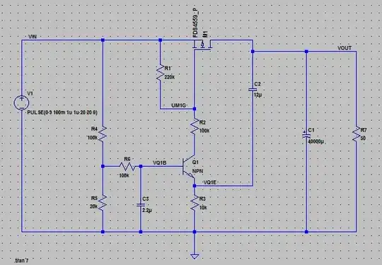
Basically, the circuit works by using the C2-R3 combination as a model (or analog) for the charging of C1. Instead of sensing the current in C1 directly, R3 senses the current in C2, and it is assumed that this value is proportional to the current in C1, which is true as long as the voltage across R3 is a small fraction of the total.

Whenever there is a drop across R3 because of current through C2, the drive to the pass transistor is reduced.

The Thevenin equivalent of the base drive to Q1 is a 1.5 V and 120 kΩ, so if the voltage across R3 ever rises as high as 1.5V - 0.6V = 0.9V, Q1 is cut off altogether, removing the drive from M1 as well. This would occur at a C2 current of \$\frac{0.9 V}{10 k\Omega} = 90 \mu A\$, which would correspond to a current in C1 of \$90 \mu A \cdot\frac{40000\mu F}{12\mu F} = 300 mA\$.

By adjusting the resistor and capacitor values, you can change that limiting current value. Note that the total current through M1 (and the power supply) is the C1 charging currrent plus the rising load current through R7, so pick the limit value accordingly.

C3 just serves to filter noise at the base of Q1. I would be inclined to make sure that the time constant associated with this (C3 times the Thevenin resistance calculated above) is less than 10% of the C2-R3 time constant. In other words, I would reduce C3 to 0.1 µF or less.


I am not sure why can we set C2 and R3 into relation to get the current through C1?

The basic equation of a capacitor says that the current through a capacitor is proportional to the rate of change of the voltage across it, and also to its capacitance:

$$i(t) = C \frac{dV(t)}{dt}$$

As I said, the assumption is that the voltage across R3 is "small", which means that V(t) is essentially the same for both capacitors. This means that the current through each is directly proportional to its capacitance.

In this specific case, the voltage across R3 can be as high as 0.9 V, which is 10% of the supply voltage, so the proportionality isn't as precise as it could be, but it's good enough for this purpose.

Regarding C3, it seems to be important to prevent an initial inrush peak due to Q1 switching "fully" on immediately. I have to choose a value above 1uF to prevent that.

Yes. I neglected to take into account the very high resistances connected to the gate of M1. These are needed in order to keep the maximum current through Q1 (which also flows through R3) to a small fraction of the C2 current, but they severely limit M1's bandwidth (its ability to switch quickly). In particular, it turns off very slowly because the gate charge must be dissipated through R1 (220 kΩ) alone.

Therefore, it makes sense that having the voltage reference (R4, R5, R6 and C3) start up slowly would help avoid that initial spike in current.

Regarding the choice of M1 — as long as it can handle the voltage and the current, and that you control the maximum VGS it sees by appropriate selection of R1 and R2, there's really nothing special required.

Pay attention to the SOA (safe operating area) diagram in the datasheet. You can plot some sample voltage and current values from the simulation in order to make sure it stays in the safe area.

Also, be sure give it an adequate way to dissipate the pulse of heat associated with the charging surge of C1 without having its temperature rise too high.

Dave Tweed
  • 168,369
  • 17
  • 228
  • 393
  • +1 clever concept - I'd not seen that done (in all my long years :-) ).. – Russell McMahon Apr 09 '15 at 15:15
  • Thank you for the explanation, very interesting. It leaves some questions though. I am not sure why can we set C1 and C1 into relation to get the current through C1? Regarding C3, it seems to be important to prevent an initial inrush peak due to Q1 switching "fully" on immediately. I have to choose a value above 1uF to prevent that. – Rev Apr 13 '15 at 08:33
  • Oh and do you have a suggestion regarding my third question? – Rev Apr 13 '15 at 08:35
  • See edit above. – Dave Tweed Apr 13 '15 at 11:50
  • Good supplement, I believe that makes it clear. Thanks! – Rev Apr 13 '15 at 12:30