Working on a PCB layout and just did some ground plane pour.
From working with tube amplifier designs I know that a good star shaped ground design helps a lot to keep hum out of the circuit. Ground loops should be avoided at all costs.
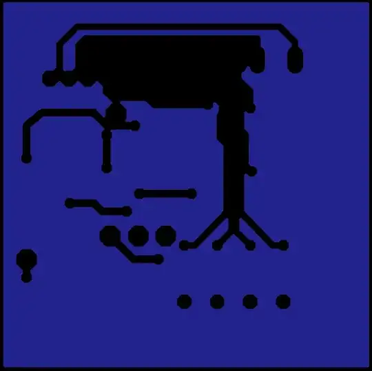
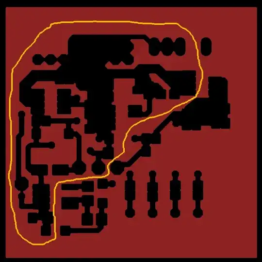
Now here is one of the ground planes of a design I'm working on. Only the ground signal is shown, other signals are hidden.

If you look closely you'll see that there is in fact a huge ground loop (shown in yellow) along with some smaller ones (not marked):
I could break the ground pour where impedance matters least and strategically place a bunch of vias to the second ground layer to get a nice star shaped ground design.
On the other hand it's very tempting to just keep the copper pour as it is and sprinkle a bunch of vias to lower the overall impedance.
What is the better way to deal with the loops? Or are such loops okay in practice?
And some additional info: The circuit itself is pure analog and contains almost entirely low impedance signals below 1kOhm. Highest signal frequency is around 10Mhz. I have very fast rise/fall times in the range of 1000V/µS though.
The circuit will likely operate in the vicinity of a 13.56Mhz RFID reader, so I expect quite a bit of RF noise.
Screenshot of the bottom layer (ground pour only):