13

Firstly let me tell you, I don't have much knowledge about the transistors in circuits. I am having a transistor S8050 D 331, and it's connected like on the schematic below. The problem I am having is when I apply input square wave signal above 300 KHz. The transistor is not following that fast. Is that normal? In data sheet it says 150 MHz transition frequency.

schematic

simulate this circuit – Schematic created using CircuitLab

Output at 100 kHz of input signal: Output at 100 kHz of input signal

Output at 300 kHz of input signal: Output at 300 kHz of input signal

Output at 500 kHz of input signal: Output at 500 kHz of input signal

Doctorslo
  • 155
  • 1
  • 1
  • 10
  • 5
    By the way, +1 for nicely documenting the question, with schematic and good measurements. –  Apr 05 '15 at 15:39
  • 1
    +1 - good documentation, as Brian says. But note too that you have "hidden in plain site" several things that need to be known for a really good answer to be possible. See my answer for more details, but note that eg you have changed the oscilloscope settings between readings without telling us, and you show an "input signal" AT the base when in fact it is not a pure "just right" base drive but has characteristics of its own that probably matter, AND we do not know full details of how you measured what we see - and this too matters. I am not trying to be over critical of an excellent ... – Russell McMahon Apr 05 '15 at 16:03
  • ... first question, but pointing out that even in apparent excellence there can be things that are less obvious than may be apparent that can affect the answer and that need to be known if the ansawers are to be complete. – Russell McMahon Apr 05 '15 at 16:04

4 Answers4

7

What they said,

BUT

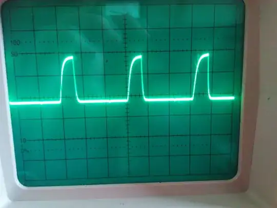
The "risetime" appears to be about 1/3 of a microsecond or more. This means that with an effective impedance of ABOUT 1000 Ohms then effective capacitance is C ~~~= T/R = 0.3 x 10^-6/1000 =~ 300 pF. Knowing how your circuit was built and the model of your scope probe and its settings become relevant at this sort of capacitance level. Whether construction is hardwired on eg vero board or on a plug in breadboard, whether you are using "bits of wire" or 100 MHz probes or ...? as probes and the brand and model of the oscilloscope all MAY matter. It is likely that the circuit itself is swamping all these effects, but they start to come potentially significant at this level.

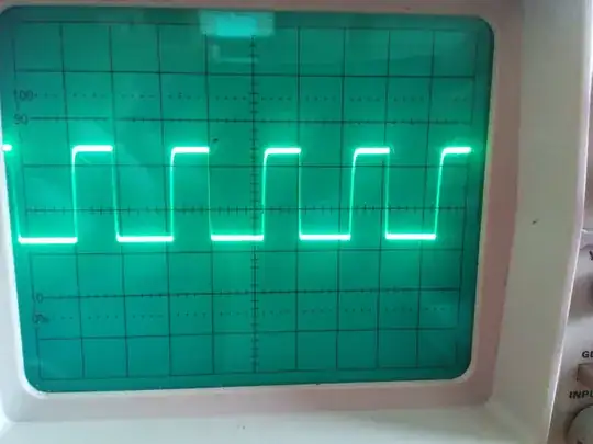
What are the horizontal (timebase - uS/division) and vertical (amplitude V/division) settings in each case?
Did you change them between displayed results? (Horizontal = yes!, vertical = maybe. See below).

The photos are useful and do a good job of showing us both what is happening AND that you are partially fooling yourself and maybe your viewers by what you show.
When you change from the 100 kHz signal to the 500 kHz signal the waveform occupies 2 divisions in both cases. This means that you have changed the timebase by a factor of 5, from 5 uS/division to 1 uS/ division. This means that the rising waveform in the first photo is 5 x slower-rising than is apparent when making visual comparisons. This makes a difference when you are trying to find out what effects are really happening and where they are occurring.

Also, it looks like you have changed the vertical scale as well, with more sensitivity in the last photo compared to the first so that it looks taller. But, this difference may be accounted for by your probe calibration.

Have you calibrated your oscilloscope probe?
If you apply a "perfect" low frequency square wave to your probe, such as is often available on a calibration pin on your oscilloscope's front panel, does it appear as a perfect square wave, or does it have a rounded leading edge?
If the probe does not let you display a square wave response to a low frequency square wave then it will mask the results at higher frequencies. Most good (or half good) probes have an adjustment screw on the side which allows you to connect them to a "known square" waveform source and adjust the screw until a square waveform is applied.
While this may seem to be somewhat cheating (by MAKING a waveform look square regardless) it is a valid operation as long as the waveform is in fact square.

And also - you do not show the driving source at the transistor base, and it matters. You will usually use a drive resistor from a source of maybe 5 volts, and this resistor value can make an immense difference to the result. A substantial improvement in frequency response can often be obtained by adding a "speedup capacitor" across the drive resistor. when turning the base OFF this capacitor acts as a divider in conjunction with the base capacitance to effectively bypass the slow resistive discharge with a capacitive voltage step. Adding a capacitor of from under 100 pF to maybe 1 nF across (in parallel with) the drive resistor may make a significant difference.

Russell McMahon
  • 147,325
  • 18
  • 210
  • 386
5

There are two things going on here, the turnoff speed of the transistor and the rise time at the end of a resistor with parasitic capacitance.

BJT's turn off slowly, especially when coming out of saturation. The circuit driving the base can help with this in two ways. It can avoid driving the transistor into saturation, and it can actively drive the base low, not just leave it floating, to turn off the transistor.

One way to avoid saturtion is to bias the transistor to near the middle of its operating range, then feed in a signal just strong enough to cause the output to go near, but not actually to, the lower limit. Another way is a Schottky diode from base to collector. This draws current from the base that would otherwise saturate the transistor when the collector gets too low.

To decrease the parasitic capacitance effect, use as low a impedance as you are willing to spend current for. For example, can you decrease the resistor values by a factor of 10 and then increase the transistor current by a factor of 10 to end up with the same voltage? If so, try that.

Olin Lathrop
  • 310,974
  • 36
  • 428
  • 915
3

You're saturating it. Reduce the base current by increasing the resistor between "Input signal" and base, so that base current is somewhere less than 10% of the collector current - try Ic/20. One trick is then to add a schottky diode from base to collector, to rob the transistor of base current when Vc < Vb. See this Q&A for more information.

0

The first reason for the bad performance you are experiencing is what other's have already said: You are saturating the transistor.

Then other reason is, you are using a very high collector resistor. Read the data sheet of your transistor. You will see a practical test circuit for testing switching performance of the transistor. You will probably see a very small collector resistor in that circuit; typically 150\$\Omega\$. The higher collector resistor you connect, the worse switching response you will get. Those fast transistors are indeed fast, but if you give enough collector current to them.

If you want to get a fast switching performance, on the other hand you don't want to waste power on a small collector resistor, I suggest you use totem pole structure or a logic gate instead.

hkBattousai
  • 13,913
  • 31
  • 114
  • 190