11

I have seen quite a bit where reverse biased diodes are used to clamp input voltages when spikes occur.

enter image description here

  • What is the typical reverse breakdown voltage for a diode used in this type of application?

It appears that these protection diodes are in place not to protect against a large applied voltage by the user, but rather are in place to snub voltage spikes that may arise from static discharges.

  • Why might a static discharge occur, where would this excess charge come from in-circuit (on a PCB, not bread-boarding where a person may introduce discharge), and what is the typical voltage magnitude?

  • Why would one not also consider the possibility of a potentially large negative voltage and also place reverse diodes from the input line to Vcc?


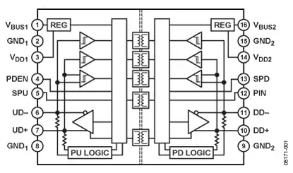
I am designing a simple breakout board for a controller that will output data through a USB interface. Through my research I found that many designs incorporate these reverse biased protection diodes on Vusb, D+, and D-, however not all do.

enter image description here

Again, if all of this is mounted on a PCB, why might a sudden static discharge occur and where might it originate?

  • How frequent is this kind of event and without these diodes is it likely to damage circuitry?

  • Is it best practice to always include these protection diodes or are they not necessary at times? If the latter, what special cases deem them unnecessary?

  • Will any diode work or should one with a specific breakdown voltage be used?


EDIT:

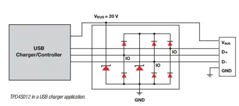
Looking over those App notes, one shows

enter image description here

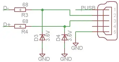
While the other shows something similar but without the "top" node connected to anything. Is this a misprint or is it implied to be connected to Vbus?

enter image description here

sherrellbc
  • 3,431
  • 6
  • 35
  • 62
  • 1
    Related app notes: [The Protection of USB 2.0 Applications](http://www.digikey.com/Web%20Export/Supplier%20Content/Wurth_732/PDF/Wurth_The_Protection_of_USB_20_Applications.pdf?redirected=1) by Wurth, [System-Level ESD/EMI Protection Guide](http://www.ti.com/lit/sg/sszb130b/sszb130b.pdf) by Texas Instruments, [ESD protection for USB 2.0 interfaces](http://www.nxp.com/documents/application_note/AN10753.pdf) by NXP. – Nick Alexeev Mar 24 '15 at 18:06
  • 1
    @NickAlexeev, Thanks for the app links. I looked them over and found something strange so I included an edit above. Little it said about the general practice except that this protection is recommended since only so much protection can be integrated into each device without increasing the required silicon area quite a bit. – sherrellbc Mar 24 '15 at 19:14

2 Answers2

8

Forget about USB for a moment, because these devices are useful in a lot more applications than just USB. First, the diodes in your first two examples would not usually be generic signal or zener diodes. They are usually purpose designed transient voltage suppressor(TVS) diodes.

TVS diodes come in all different flavors, but there are three key parameters. First, the maximum reverse standoff voltage. This is the working voltage. For USB, you'll want to be very close to 5V. The next thing you'll want to look at is the clamping voltage. Again, around 5V for USB. Usually, the leakage current rises significantly as the clamping voltage approaches the reverse standoff voltage. Be aware of that in case it matters in your application. The last key parameter is the peak reverse current. Make sure it can handle the standard you're going to test against.

There is one more thing to be mindful of when placing TVS diodes on high speed signal lines (ie. USB, HDMI, Ethernet, etc). Make sure the TVS diode is low capacitance. There a many diodes and arrays suited for this purpose and will have capacitances in the neighborhood of 0.2pF.

I'm going to skip straight to your second example since we're talking about USB here. The scheme shown would be appropriate if the diodes shown clamp around 5V, and are trying TVS diodes. Regular zener diodes are not fast enough for ESD protection.

In your last example, you question whether the top node is connected to Vbus and according to the device datasheet, it is not. If a positive ESD event occurred on any of the signal lines, that TVS would clamp it. The Vbus TVS has a higher clamping voltage for the power rail.

Matt Young
  • 13,734
  • 5
  • 34
  • 61
7

You asked,

Again, if all of this is mounted on a PCB, why might a sudden static discharge occur
and where might it originate?

The potential problem is ESD (Electrostatic Discharge) originating from outside the PCB, coming in from the USB connector. A user might be carrying a product across a carpet or other ESD-generator, and touch the USB connector with their finger. Even if there is a cable plugged into the USB connector, they might touch the connector at the other end of the cable and pass thru USB.

This is true not only for USB connectors, but any connectors coming out of a product -- even the power jack.

When we design a product for sale, and have it tested for EMI/EMC (Electromagnetic Interference and Compatibility), the testing house injects brief 8,000V (8kV) low-current spikes on to each of the connectors, and afterwards tests that the device still functions correctly. The devices shown in your schematics are designed to protect against discharges of this level or higher. Without the ESD protection, it is likely the device would fail this test.

Why get UL certification, which can cost thousands of dollars at a test lab? Is it a legal requirement? No, but a lot of retailers such as Walmart won't carry electronic products unless they have a UL label. In Europe, the equivalent is the CE mark.

tcrosley
  • 47,708
  • 5
  • 97
  • 161