-1

I have a partial discharge wave form which varies between -100mV to +100mV. For simplification, I am using a sinusoidal wave with that range. I need to amplify and bias this signal between the range of 0-3.3V since this signal will be an input to the arduino. I have looked into instrumentation amplifiers and tried to simulate this on multisim but I am not getting the desired result. Can someone help me with this design? Thank you.

EDIT:

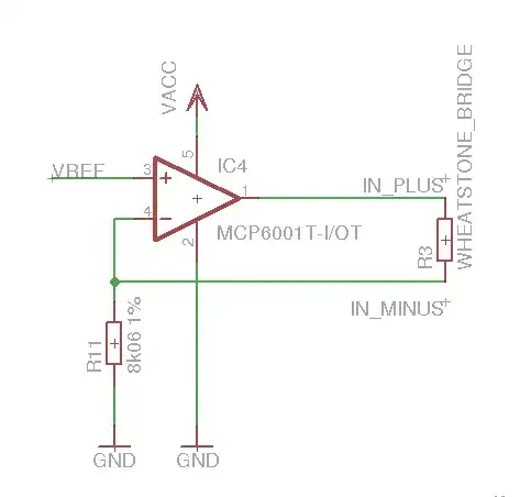
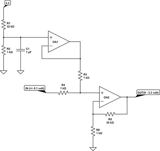
This is the complete circuit that I tried to draw (I got this circuit off the internet from my research - i do not have the link). I am trying to bias the input ( input is 100mV peak sine wave centered at 0. I want bias to be 1.65V). This is not the instrumentation amplifier since this is the first circuit I tried to model without the use of an in-amp.

So basically, the circuit involves and input sine signal, a bias, buffer and an non inverting amplifier (the last op-amp at the bottom)

enter image description here

enter image description here

enter image description here

enter image description here

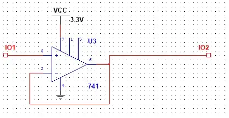
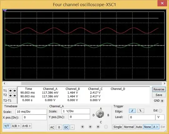
Second image is the subcircuit Op-Amp 1. Third image is the buffer. From what I know you would need a buffer to match the input and output impedance The last image is the oscilloscope.The green waveform represents the input signal. The red is the output from the buffer. It is biased around 1.65 volts. But when I add the non-inverting op amp, I get a straight line on the oscilloscope (represented white on the oscilloscope)

Also, all the op amps are single rail.

Uzair
  • 1
  • 2
  • "Not getting the desired result" is not sufficient for telling us what problems you are having. What about the sim isn't working? What components did you try, do you have a circuit diagram? – Paul L Mar 14 '15 at 19:11
  • I added some more details, I hope it makes sense. I am new to this forum so sorry about the lack of details in the question. Thanks! – Uzair Mar 14 '15 at 19:43
  • What is the frequency? Coupling with a cap can shift an AC signal. – C. Towne Springer Mar 14 '15 at 23:44

3 Answers3

1

Perhaps you are trying to level shift and amplify like here? Analog voltage level conversion (level shift)

1

1) User2604188 points in the right direction, although it's not a perfect answer in this case.

2) Your R1/R2/R3/R4 network will not work as you think. R1/R2 does provide 1.65 volts, but this gets loaded down by R3/R4. When Vin is 0 volts, the output level is 1.32 volts. Not only that, but the output voltage swing is only 40% of the input, so you'd need more gain than you think.

3) The primary reason your last op amp doesn't work the way you want it to is that its gain is referenced to ground. Your buffer output (the red trace) has a minimum voltage of ~1 volt. Your non-inverting op amp has a gain of 3. So the smallest output you can expect from your circuit is about 3 volts.

4) Given that your op amp is trying to put out about 3 volts, why is the output flat at about 2.5? That's simple - a 741 is not capable of operating at +/- 3.3 volts, let alone single supply at 3.3. Multisim makes an attempt to model a 741 which breaks down rather badly when the amp is run way outside its nominal operating range, and in this case you cannot trust its output. It's telling you that the op amp is trying to drive high, but cannot go anywhere near 3.3 volts.

I don't know what op amps Multisim supports, but I'd suggest you try something like an LTC6255 or AD8651. Then

schematic

simulate this circuit – Schematic created using CircuitLab

will more or less work. Note that the output is affected by noise on the 3.3 volt line, and depends on the 3.3 being exactly correct at all times, which is not a good assumption.

WhatRoughBeast
  • 59,978
  • 2
  • 37
  • 97
0

schematic

simulate this circuit – Schematic created using CircuitLab

This simple circuit should work. The first stage should amplify the input voltage two times and also translate the input to 0-400mV range. The next resistor capacitor phase I have used basically to ground your low frequency DC to enhance your signal clarity. The R and C values should be decided by you depending on where you want your cut-off to be. The third stage I have designed to be a simple amplifier. You just need to calculate your R5 and R6 values. They should not be too complicated. According to my calculation the ratio of R6 to R5 should be less than 7.25. I think this should work well for your case.

ubuntu_noob
  • 656
  • 1
  • 7
  • 22
  • You might want to rethink your circuit. Wrong choice of op amp for single supply 3.3v operation. C1 eliminates the offset you introduced. Direct coupling of C1 to OA2 will cause uncontrolled bias drift. TL081 is not rail-to-rail output. – WhatRoughBeast Apr 15 '15 at 10:25
  • No, I didn't look into Op-amp choices, 081 is the default in the simulator. LT1366 is a good choice or maybe even 1677 – ubuntu_noob Apr 15 '15 at 11:09
  • 1
    Yeah, but the other problems remain. And there's one more problem. Even if the runaway drift problem on OA2 is fixed, the output remains bipolar, and will not be in the range 0 - 3.3. – WhatRoughBeast Apr 15 '15 at 11:16