5

Is it possible to put a via right next to the component pad it is connected to? In other words, if a via and a component pad are on the same net, can they touch as in the image below (red=top layer, yellow= mid layer, gray=via's pad, brown=hole, pink=component outline,distance shown=edge of hole to edge of pad)?

enter image description here

aghoras
  • 425
  • 6
  • 12
  • 1
    Is it possible? Yes. You can even put plated holes in the middle of pads (I've done this for heat sinking). It can cause issues with solder since it will wick the solder down into the via before flowing on the pad, I worked with my manufacturer to make sure solder was ok on my boards. If you're hand soldering really not an issue at all. – I. Wolfe Mar 12 '15 at 14:55
  • What about a via under a pad? After a (GND)polygon pour, I had an isolated GND island. The only way out was a via directly under a pad. By the way I will solder the components manually. – Bence Kaulics Mar 12 '15 at 15:17
  • 1
    you might want to add some copper, either a trace or tiny flood to cover the triangle formed on the left hand side where the via meets the pad. I've seen fab houses flag that as a distance violation before. More annoying than a real issue but save yourself the trouble. – Some Hardware Guy Mar 12 '15 at 15:37
  • 1
    @BattleHamster - As long as the via and the pad are on the same net, that's no problem. Just make sure when you solder the component on the pad that the via gets filled and the component is soldered sufficiently. If you are reflowing it can become an issue, but if you're going to use a soldering iron I wouldn't worry about it – I. Wolfe Mar 12 '15 at 15:39

3 Answers3

6

This is another, yes it can be done, but think about it carefully thing. Usually if you put a via in or close to a pad, it is going to an internal plane. Not having a trace between the via and pad will provide the lowest impedance path to the plane. It also helps to put several small vias in parallel. There's a problem with doing this though. Having a hole in the pad is going to wick solder off the pad, into the plated via. The smaller the vias the better, but you need to evaluate whether that is a problem in your application.

From the image you posted, I don't think I would put a via that close to that pad. It's going to a trace on another layer. There's no reason to try to minimize the via impedance there. If space is the constraint, try making the via smaller, and the pad if you can afford it.

Matt Young
  • 13,734
  • 5
  • 34
  • 61
  • See also the many posts at http://blog.screamingcircuits.com/via_in_pad/ about vias in pads. – hlovdal Mar 12 '15 at 15:24
  • +1, and if you're going to do via in pad then you should consider non-conductive fill and plate flat. – Some Hardware Guy Mar 12 '15 at 15:35
  • My hands are tied: This is a 10 layer board so I can't make the hole smaller without violating the minimum aspect ratio. I can't make the pad much smaller because it is for a 0603 sized part and I'm afraid enough paste wont get on pad. Also, there is not enough room to move the via further away. What I'm trying to figure out is whether it is worth the effort to re-layout that section of the board or can I just leave it as is. I forgot to mention: the board will be assembled by a machine and reflowed. – aghoras Mar 13 '15 at 13:17
  • @aghoras You can push the via, and trace above it up .015 without re-laying out everything? – Matt Young Mar 13 '15 at 13:22
  • Not really without breaking my via-pad to trace clearance rule. You can see how the red trace is bowed up already. – aghoras Mar 13 '15 at 15:09
  • @aghoras Yes, but we can't see what is above that. – Matt Young Mar 13 '15 at 15:10
4

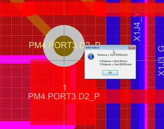
Remember that the registration of the drill holes to the copper features will not be perfect. Typically the drill hole center might wander by 4-10 mils from the location you drew it at.

Usually we choose the size of the copper ring around the pad so that with maximum offset of the drill center, no more than maybe 25% of the perimeter of the drilled hole will be outside the pad.

If your hole registration and via pad are designed this way, in your diagram that means the drilled hole could end up with about half its area within the square pad.

If you are designing for mass production, I would not recommend this design. I'd rather either move the via far enough away from the pad to ensure there's a soldermask dam between the pad and the via, or pay for via-in-pad-plated-over (VIPPO).

The Photon
  • 126,425
  • 3
  • 159
  • 304
1

I strongly recommend against doing this. If you put a via so that it touches a pad, it will cut off some of that pad. It will make soldering more difficult and could even lead to poor connections. It would cause unevenness and the component may not sit properly. Some board houses may not even allow this at all. I urge you to try to avoid it.

DerStrom8
  • 21,042
  • 8
  • 61
  • 95
  • 2
    A good board house will make whatever you send them, as long as it is within their capabilities. It isn't their job to save you from doing dumb things, and if you design something that can't be easily assembled, that is on you. – Matt Young Mar 12 '15 at 22:42
  • 1
    @MattYoung A fair point. I just know that some board houses have clear-cut rules for component/via/trace clearance – DerStrom8 Mar 13 '15 at 02:30