I am designing a PCB layout in Eagle and in the datasheet of my modul it is said that "Non solder mask defined (NSMD) type is recommended for the solder pads on the PCB". Does it mean that there will be no solder on pads? By default pads are enabled for tStop and tCream in Eagle. Should they be ON or OFF in this case? How can arrange this situation in Eagle?
Asked
Active
Viewed 5,629 times
5
Splendor
- 51
- 1
- 3
2 Answers
10
Does it mean that there will be no solder on pads?
No, it means there will be no solder mask on the pads.
I don't know about Eagle terminology / settings, but in the software I use this is the equivalent:
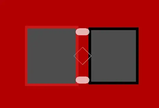
(Key: red = solder mask, grey = copper pad, black = substrate).
The pad on the left is "mask defined" in that the area of the copper in the exposed pad is entirely defined by the aperture in the solder mask. The pad on the right is not "mask defined" in that the copper area is smaller than the solder mask aperture.
The point of this is to prevent the solder mask causing a rise in the overall height of the pads at that location which can cause the module to not sit flat or make good contact with the pads after reflow.
To further illustrate, I have taken your existing picture and depicted what can happen with the two pad layouts:
In the left hand pad the distance between the component and the pad is limited by the thickness of the solder mask. Unless there is the exact amount of solder paste available the pad won't be soldered reliably as there isn't enough solder to fill the gap. Voids are formed and a bad connection may well result. With the right hand pad the solder paste is able to pull the component all the way down to create a proper clean sandwich of solder between the two pads resulting in a much more reliable connection.
Majenko
- 55,955
- 9
- 105
- 187
-
logic is very well explained, thank you. I think NSMD is the default setting in Eagle – Splendor Mar 11 '15 at 15:57
-
1I would be surprised if it wasn't - all the programs I have used have been NSMD by default. – Majenko Mar 11 '15 at 15:59
4
It means they want the pad outline NOT defined by the solder mask edge, but instead by the edge of the copper. I don't know why they are making a big deal of this, since this is the usual case anyway.
Note the difference between your left and right pictures, which is whether the solder mask protrudes over the copper area or not. The right case is the norm, and you specify that in Eagle by one of the clearance values in the package definition.
What they don't want you doing is to make the copper larger than needed, then have the solder mask overlap it to define the actual pad area. You should normally avoid that anyway, since the solder mask has some thickness, and the pin may therefore not be in direct contact with the copper.
This is a bit like your car owner's manual warning you that when you fill up with gasoline, to make sure you don't pour the gasoline in the trunk, and that it should go into the gas tank instead. Of course you're going to do that, so mentioning it causes more confusion because you wonder why they even brought it up and what you may therefore be missing.
Olin Lathrop
- 310,974
- 36
- 428
- 915