2

I am trying to simulate an RS master slave flip-flop in Logisim, and I have encountered the "Oscillation apparent" error. What does this error mean and how is it resolved? I am required to use two nor gates for the basic RS latch implementation and two of the basic latches with a clock signal for the master slave flip-flop.

RS master slave flip-flop

RS master slave flip-flop

RS flip-flop (latch)

RS flip-flop (latch)

Fizz
  • 14,355
  • 2
  • 43
  • 97
Patrick Taylor
  • 31
  • 1
  • 1
  • 2

3 Answers3

1

Many kinds of latching circuits are prone to starting up in an ill-defined state. In your nor-based RS latch, if on powerup both inputs are low and the gates are assumed to output low, then all the inputs to both gates will be low, so the gates will output high. Then since each gate will have an input high, both will output low, etc.

A nice approach to the problem, if you're allowed to use it, would be to have one of the NOR gates of each latch take three inputs, and wire the extra input from both of them to an "asynchronous reset" signal which will be pulsed high on simulation start-up. Otherwise, it will be necessary to ensure that both of your latches get clocked soon enough after simulation start that the simulator won't squawk at the oscillation.

supercat
  • 45,939
  • 2
  • 84
  • 143
1

This is a D-FlipFlop that I made in Logisim. It uses only transistors and Pull Resistors. All three of the In Pins are set on Pull Down. Logisim tends to agree with this logic more because it weeds out error signals. the oscillation errors will still be there unless delays are placed at certain points in the subcircuit. There is also normally a glitch that can be apparent which is one and two tick pulses. These can be removed by placing "pulse correctors" as I call them. The two things placed at the Q out and the Clk In Pins are pulse correctors. If you don't understand a part of it, experiment around with it. Speaking from personal experience, you learn more if you figure it out by yourself.

D-FlipFlop

jbarlow
  • 1,593
  • 9
  • 15
Legoking
  • 11
  • 1
  • 3
    Welcome to EE.SE. Your answer doesn't seem to effectively address the question and is unclear to me. Can you improve your explanation? Additionally, your circuit diagram is very unclear, particularly because you have put the logic high supply and a resistor between almost *every* transistor. – user2943160 Jul 30 '16 at 02:04
0

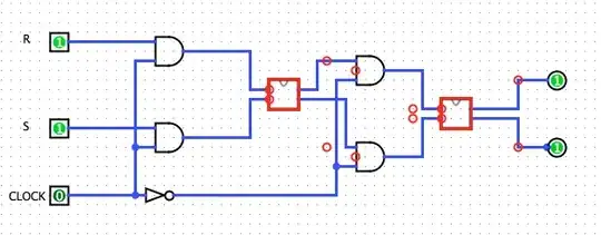
It looks like your latches are not clocked.

A clock signal needs to go to each of the red squares. For a rising edge master slave flip flop, the master latch (first latch) needs to be transparent when clock is low. The slave latch (second latch) needs to be transparent when the clock is high. So, give the first latch inverted clock, and the second latch clock. Invert this and you will get a falling edge triggered flip flop.

Here are two ways.

Not sure if you want to use the extra AND gates to synchronize the SR portion.

rs master slave synched

If not you can save the gates:

rs master slave

There might be other ways to do it.

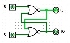
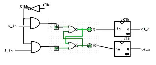
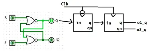
The SR latch is asynchronous to clock, it changes whenever inputs come. The outputs are synchronized with the latches. During the low clock phase, the first latch is open. Q from the RS latch is transparent. Once the clock rises, the first latch closes, and holds its internal state. At the same time, the second latch becomes transparent. It takes the value from the first latch and pipes it to the output. Since the first input was R (the way I have it hooked up), the R signal is produced at o1_q during at the rising edge. Its inversion is S.

jbord39
  • 4,320
  • 1
  • 17
  • 25