3

enter image description here

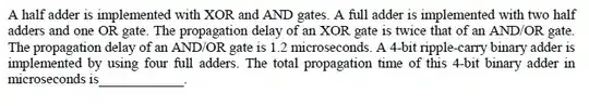
In pic below I have drawn a full adder and mentioned their delays, please help me to verify my answer.

enter image description here

Vikrant Singh
  • 133
  • 1
  • 1
  • 7
  • Hi and welcome to eesx. Homework questions are **not** off topic here but please add some insights on what you have done till now. Just drop some photos of the half adder and full adder you have drawn, and how you would connect the adders to make a bigger adder. – Vladimir Cravero Feb 11 '15 at 09:35
  • This is not the home question, this has been asked in GATE 2015 Computer Science exam for admission in Post graduate program. for LSB bit I used one half adder and for remaining 3-bits I used Full adders, delay for one half adder sum Si = 2.4 us and carry Ci+1 = 1.2 us. delay for one full adder sum Si is 4.8 us and carry Ci+1 = 3.6 us After that I got 16.8 us as delay. – Vikrant Singh Feb 11 '15 at 10:12
  • First of all you should use only full adders, as stated in the problem text, your delay will then be one sum to carry plus three carry to carry. – Vladimir Cravero Feb 11 '15 at 10:31
  • is 19.2 us is correct answer? – Vikrant Singh Feb 11 '15 at 10:40
  • I do not know. Either you provide some drawings of what you have done or I'm not gonna dig in this. As I said homework questions are **not** off topic but low qualities questions are. And yep that's an homework question also if you're not doing your homework. – Vladimir Cravero Feb 11 '15 at 10:42

2 Answers2

2

Your analysis of the single full adder is correct as far as it goes, but it is incomplete.

The delays you show are all based on the Xi and Yi inputs. But the delays from the Ci input are different, since they don't go through the first half adder.

The reason this is important is that when you combine the full adders together to create a 4-bit adder, the Ci to Ci+1 delay is a key component of the "critical path" to the upper output bits and the final carry output.

When doing this sort of timing analysis, you need to consider the delays from each input to each output, and use the appropriate delay when combining modules together to form larger structures.

Dave Tweed
  • 168,369
  • 17
  • 228
  • 393
  • So what is the answer according to you? – Vikrant Singh Feb 11 '15 at 12:17
  • Really? You're not going to try to work it out on your own first? All right, I'll tell you that the total delay from `X0`/`Y0` to `C4` is 12.0 microseconds. Can you work out the delays for all of the other outputs? – Dave Tweed Feb 11 '15 at 12:26
  • sorry sir, C1 will be out by 0+4.8 = 4.8 us C2 will be out by 4.8+2.4 = 7.2 us C3 will be out by 7.2+2.4 = 9.6 us C4 will be out by 9.6+2.4 = 12 us this is what i get, please verify this. – Vikrant Singh Feb 11 '15 at 12:31
  • Yes. And what about the delays to the S0, S1, S2 and S3 outputs? – Dave Tweed Feb 11 '15 at 16:13
1

It took me a while but here's how it is :

The first carry and sum will be available after 4.8 us. This should be straight forward.

However, for the subsequent stages, you need to keep in mind that the output of half adders is already there at 2.4 us. So in a sense, it is already computed. The remaining half adder for each full adder is just waiting for the previous carry, which when available from the previous stage can be processed in 2.4 us. So each next stage will take only 2.4 us each.

The catch here is that half of the output in each next stage is already computed, only half needs to be processed.

Plutonium smuggler
  • 1,391
  • 2
  • 19
  • 32