0

Trying to figure out how the BJTs would affect the following circuit:

bjt

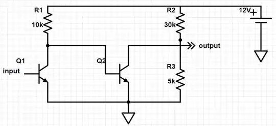
I'm confused overall, but some specific questions include:

  • If the input is off, the first transistor is effectively off, and VC1 = VB2 ~=12V. This sets the gate of the second transistor to be on/saturated (as the 0.7V needed across VBE2 is present). But how does this affect the output?
  • Does the voltage divider of the 30k and the 5k force 1.71V at all times on the output, regardless of the input?

Thanks for any/all help and clarification!

EE_padowan
  • 31
  • 1
  • 3
  • 1
    Is this homework / assignment etc. That can be acceptable but you must say. |You say Vb2 = 12V and VBE2 = 0.7V - are they not the same point? If not, define them. When Q2 is saturated what is its effective resistance compared tp R3. What does that make of your statement re 1.7V out at all times? – Russell McMahon Feb 10 '15 at 05:15
  • With the output transistor saturated, you will not get a signal output, just a very low DC voltage. – user66283 Feb 11 '15 at 21:31
  • You should correct your schematic. I assume the output of Q2 is connected to R2 and R3 but currently there is no junction there. Don't just move the dot down, as four way junctions [are discouraged](http://electronics.stackexchange.com/a/28255/1322) #11 -- there should be two T junctions instead, with one dot on each. You should also correct the junction below Q2 as well. Furthermore, you are missing a dot above R2. I know I'm being picky, but you might as well get into good habits. – tcrosley Feb 12 '15 at 00:33

2 Answers2

1

When Q1 is off Q2 turns on, (with Q2's "base" at 0.7v), and the output line goes low, (near 0v).

When Q1 is turned on Q2 turns off, and the output returns to the voltage determined by the resistor divider.

This is assuming the ouput line connects at R2-R3, as your connection dot is shown offset.

Nedd
  • 7,939
  • 15
  • 19
  • A few extra notes: It is more traditional to write collector voltage as "Vc" rather then VC. For example using VC1 might be taken as voltage on a capacitor listed as C1. Similarly for a transistor's base voltage "Vb" is preferred, as VB2 might be confused as voltage on a battery shown as B2. Lastly, in this circuit Q2 is not necessarily saturated since saturation implies that the transistor has a high enough base current to allow the collector current to be flat lined (near its maximum). – Nedd Feb 10 '15 at 05:33
  • When using a first approximation of a transistor it is often assumed that Vce at turn on is 0v. But at a higher level approximation (dependent on the transistor's spec sheet) Vce is not really at absolute 0, (though that would be quite cool...). Above and below saturation Vce actually has some value above 0v. (In saturation Vce is lower.) This action is like a small value phantom resistor in series with the collector. This phantom resistor's value could be calculated by looking at a chart comparing the transistor's Vce voltage to the collector current (Ic) at a certain level of base current. – Nedd Feb 10 '15 at 11:00
  • Yes, sorry - good catch. R2, R3, output, and Q2's collector pin are all connected. – EE_padowan Feb 10 '15 at 15:14
0

No, transistor Q2 is turned on, so provides a parallel resistance to the 5K resistor. So Vout = (12V x Rp)/(R2 + Rp) where Rp = (R3xRon)/(R3 + Ron). Ron is on resistance of Q2. Also VC1 is clamped by base emitter diode of Q2, approximately .7V. Current limit is provided be R1.