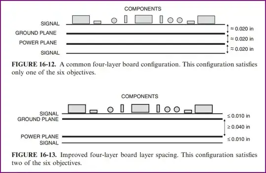
The increased spacing in the middle lowers the effectiveness of plane capacitance which depending on your application may or may not be useful to you.
The decreased spacing from signal to plane will let you use thinner traces to achieve similar impedances, while reducing the effect of cross talk between signals (assuming the same trace to trace spacing in each Stackup). The closer to the plane the more contained your field will be and you should also see less radiation. You can see this effect nicely in say hyperlynx if you have access to it ( or others they just draw nice field lines)
Given the choice I would go with thin dielectric for outer layers usually 3-5 mil for me, vs thinner spacing between the inner layers.
Editing to add:
I'm just talking SI/PI here. Increasing the inner core thickness to 100 mil will also increase the length of your vias, which increases their inductance and reduces their effectiveness at pulling current out of your planes as frequency goes up. So it has the effect of increasing the inductance of decoupling capacitors (assuming you're using vias to connect your caps to planes), as well as your package to plane connection. Basically the increased distance with all other things being equal will have worse power integrity. It doesn't mean you can't do it but that's an effect and if it's a concern you'd have to understand the consequences before increasing the thickness. You could mitigate it for example by adding more vias.