2

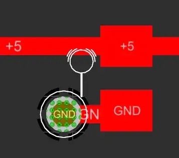
I just started routing my first PCB on Altium. It is a simple 2-layer board with bottom layer as dedicated GND plane. I started out placing GND vias for GND pads of the top layer SMD components like this:
enter image description here

But Altium gives me a "Net Antennae Violation". The Altium documentation states:

This rule operates at a net level in the design to flag any track or arc end that is not connected to any other primitive and thus forms an antenna. The specified value is the set tolerance of how long a stub must be before the rule will flag an error. Default for this rule is set to 0.

So I understand that a Via is no primitive and I could just disable the design rule. But I would like Altium to still warn me about something like this
enter image description here

while suppressing the GND via antennae violation.

Is there any way to achieve that?
Rev
  • 10,017
  • 7
  • 40
  • 77

3 Answers3

3

Every time, when I am about to finish my PCB layout, I get this warning of 'Net Antennae'. But, the solution is simple:

You need to re pour all the polygons before you run the design rule check. In this way the violation does not appear.

Theta
  • 51
  • 3
1

I think this is because you do not already have a ground plane below it? Also make sure your ground plane is on the correct net (ie, set the ground polygon to GND net). BTW, I just tested this using a "Solid Region" as my ground plane.

enter image description here

Nate
  • 334
  • 2
  • 11
  • The GND plane is there but I used a Polygon Pour since I want it to pour around THT pads and other obstacles (which is common for power/GND plane IMO). You can see the thermal pad connections in the first picture (dimmed out though, thus gray). You are right that using a "Solid Region" prevents the error (it is probably treated as a primitive in contrast to the "Polygon Pour") but it does not really help me since it would be kind of a "dirty" workaround. Thank you anyway for your feedback. – Rev Feb 03 '15 at 08:19
  • did you try going back to the bottom layer and double clicking the poly? I just got this to work with a poly pour by (1) creating the pour and setting it to GND net (2) creating a trace off a ground pad (3) placing a via, setting it to GND net then (4) going back to bottom layer and double clicking poly to rebuild it. No net antennae violation. – Nate Feb 03 '15 at 08:49
  • I think it was some kind of bug. I deleted the existing polygon, placed a fresh one and now it works. I would say that everything is set up exactly like it was before. Since I did a lot of wild clicking and testing in this first design, maybe I somehow screwed it up. Thank you for verifying. – Rev Feb 03 '15 at 08:56
  • This was my issue. My RGE VQFN package describes a grounded "Thermal Pad" in the center. I added a large rectangle pour to the side opposite the chip, connected it to ground, and the warnings went away. Hoping the manufactured board works :) – nialsh Oct 07 '16 at 16:35
1

You may have a "hidden" track segment.

Click on the Via and on the track and on the pad. Check the multi-selector box carefully. There is probably an extra segment hiding in there that is causing the violation.

DrFriedParts
  • 12,482
  • 36
  • 54
  • This came to my mind as well, but there is no hidden segment and since I got the error for every via of this kind it was unlikely. – Rev Feb 03 '15 at 08:22
  • JFYI, either it was a bug or I messed it up at some point. See comment on the other answer. Just placing a new polygon helped. – Rev Feb 03 '15 at 08:58
  • Excellent! Glad to hear it worked out for you. :) – DrFriedParts Feb 03 '15 at 16:24